


By Peixun Fan and Minlin Zhong
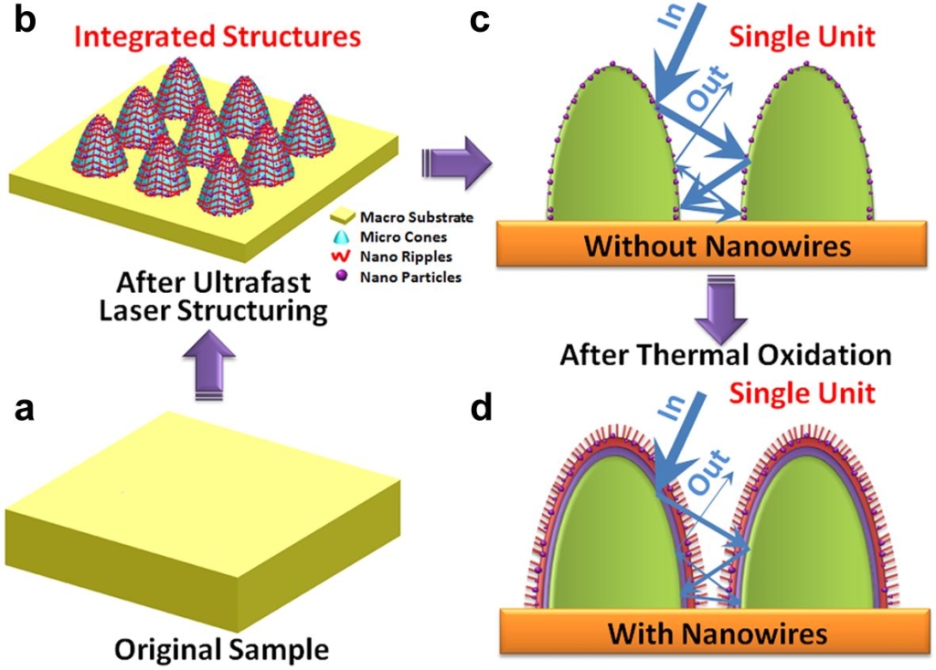
Infrared antireflection surfaces are of great realistic significance in wide fields including infrared imaging, sensors, thermoelectrics, stealth, artificial blackbody, etc. However, efficient infrared antireflection property still remains a major challenge, especially on metal surfaces which are usually inherent excellent reflectors at the infrared wavelength regime. Until now, few reports of near unity infrared AR property reaching reflectance below 1 percent and fewer reports of broadband near unity AR strategies which keep effective through the spectrum of 5~25 μm on metal surfaces have been demonstrated. It is known that the high optical impedance between metal and the free space is the culprit accounting for the severe apparent reflection of metal surfaces. An effective method for alleviating the optical impedance is to introduce a transitional medium. The semiconductor materials, metal oxide in particular, are expected to be good candidates to realize such a purpose. However, it’s technically difficult to steadily produce a uniform as well as highly efficient oxide layer on metal surfaces. Here, we propose a novel ultrafast laser hybrid processing approach to tackle this fundamental challenge. By forming precursor micro-nano structures via ultrafast laser, oxide in the unique structural form of nanowires is facilely and uniformly grown on Cu surfaces after a subsequent simple thermal oxidation process.
Figure 1 shows the scheme and strategy used in our approach. We use an ultrafast laser to produce specific micro and nano structures on Cu surfaces first. After that, the Cu samples with micro-nano structures were heated in a furnace in static air for thermal oxidation, through which oxide nanowires are expected to grow along the skins of the laser produced micro-nano structures. The bulk Cu substrate, the laser fabricated microscale structures and induced nanoscale features, together with the oxide nanowires, construct a unique macro-micro-nano-nanowire hierarchical structure. The relatively large-scale Cu micro structures serve as the skeleton of the whole surface architectures, which can play the role of geometrical light trapping and induce multi internal reflections to some extent. Meanwhile the nanowires together with the oxide layer surrounding the micro structures constitute the transition medium from Cu substrate to the free space. Comprehensively, highly efficient antireflection performance can be achieved.
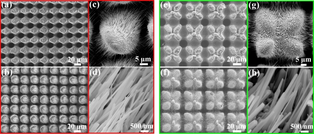
The macro-micro-nano-nanowire hierarchical structures, as well as their antireflection properties, can be facilely tuned through simply control the laser processing procedure. For instance, we have produced micro cone as well as micro petal arrays on Cu surfaces, as shown in Figure 2. Oxide nanowires are successfully produced on both kinds of micro structures after thermal oxidation regardless of the structure morphology. The nanowires grow radially out of the outer surfaces of the laser produced micro structures to the free space with a dense and uniform distribution, reaching a length over 10 μm.
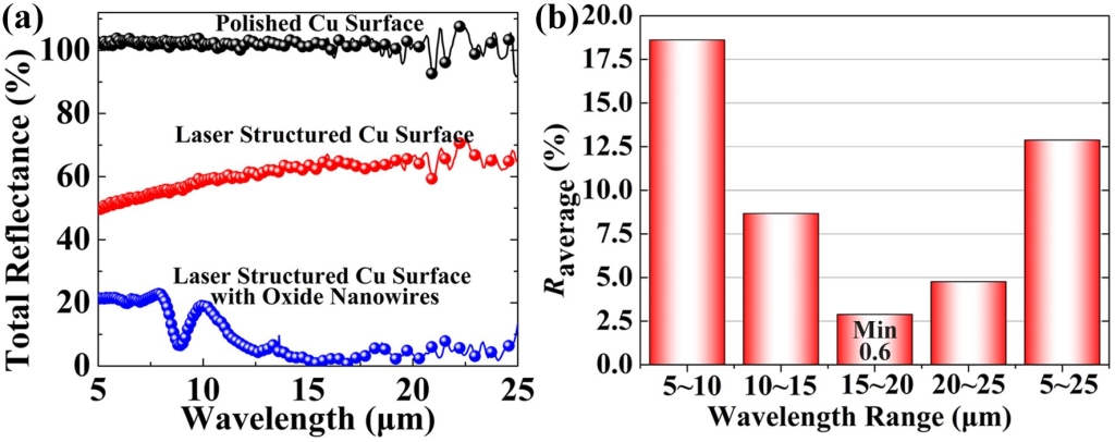
The antireflection properties of the above hierarchical structures in the mid-IR region have been measured, as shown in Fig. 3a. The polished Cu surface without any antireflection structures displays high reflectance throughout the mid-IR regime. With ultrafast laser fabricated micro-nano structures, the total reflectance of Cu surface shows a 20-30 percentage-point decrease compared to the polished one. After further growing nanowires, the total reflectance of the Cu surface declines abruptly over the whole studied spectrum range, and some deep reflectance valleys emerge. In particular, the surface reflectance drops to a minimum value of ~0.6 percent at around 17 μm, which is the least experimentally realized result reported to date on metal surfaces, to the best of our knowledge. More importantly, this near unity infrared antireflection property is not obviously wavelength sensitive, namely, it’s a broadband spectrum feature with the total reflectance kept steadily below 3 percent over the range of 14~18 μm. Since the bulk Cu substrate is opaque at the infrared regime, this corresponds to a 97 percent absorbance. Figure 3b further demonstrates that the arithmetical average of the measured reflectance within the 10~15 μm, 15~20 μm, and 20~25 μm regimes are all lower than 10 percent. Even from the perspective of the entire studied spectrum range from 5-25 μm, the broadband infrared antireflection properties maintain effectiveness, with a notable low value of 12.5 percent being reached. This indicates that nearly 90 percent of the surface reflection has been successfully eliminated via the unique macro-micro-nano-nanowire hierarchical structures.
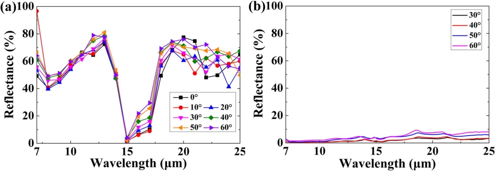
Due to the isotropic and symmetric distribution of the large-scale Cu micro structure arrays, this broadband near unity infrared antireflection property shall be free from any angle or polarization sensitivity. Correspondingly, the total reflectance of the macro-micro-nano-nanowire hierarchical structures at oblique incident angles has been simulated and the specular reflectance has been experimentally measured. Figure 4 shows that neither the simulated total reflectance spectra nor the measured specular reflectance spectra have shown any apparent change as the incident angle increases to even 60°. Thus, it demonstrates that the fabricated hierarchical structures in present study can show unique infrared antireflection property independent of the angles of incidence.
The macro-micro-nano-nanowire hierarchical antireflection structure demonstrated here requires no conventional nanofabrication techniques (e.g., lithography, wet etching), and thus can easily be implemented to cover a large area. Furthermore, the nanowires are under protection of the microscale skeletons, avoiding any durability concerns. Both the highly ordered large-scale micro structure arrays and the in-situ grown nanowires can be reproduced conveniently, enabling its use as a reconfigurable system. The material simplicity, the structure robustness as well as the architecture reconfigurability represent significant advantages for practical usage. Additionally, the combination of the microscale skeleton with the nanowires provides us more tunable variances for achieving desired antireflection performance in desired spectral ranges. Therefore, we believe the presented methodology should also be effective for the THz, microwave and other low frequency regimes. Finally, our approach provides a general and convenient route for assembling different kinds of materials to a variety of building blocks with novel structures and functions. In particular, it should be universal to the integration of other kinds of semiconductors with metal substrates for wide applications in light management.
Peixun Fan and Minlin Zhong are with the Laser Materials Processing Research Centre, School of Materials Science and Engineerin at Tsinghua University in Beijing, PR China.