


By Debbie Sniderman
A new class of semiconducting materials, 2D transition metal dichalcogenides (TMDCs), have exceptional optoelectronic characteristics and can be made ultra-thin. When reduced to a few or mono-layers, they have the potential to meet the small size, high mechanical stability and low power requirements, and be integrated into flexible electronics and used as an alternative material to conventional silicon-based electronic devices.
TMDCs are inorganic semiconductors that have a transition metal and one other element with the chemical formula MX2 (M=Mo, W; X=S, Se, Te). Their relatively large bandgap, fast response and ability to absorb light makes them interesting for very sensitive sensors for biological detection, light sensing, fast switches and photo detector and solar cell applications.
Thin layers of these crystals are formed by processes that do not produce films of uniform thicknesses, and at the ultra-thin or few monolayer levels, multiple layers are held together by Van der Waals interactions. So handling, processing and making transistors out of these materials is sensitive and delicate compared to bulk materials or even films of tens nm thicknesses. The main goal of Dr. Costas Grigoropoulos’s research at the University of California Berkeley’s Laser Thermal Laboratory is to establish reliable and stable processes for fabricating high performance devices using these ultra-thin layers.
Stable Site-Selective Doping
Creating ultra thin layers of TDMCs is difficult, and current processes such as exfoliation or CVD synthesis don’t produce films with uniform thicknesses. “That’s a major roadblock in getting these materials to have a wider application use,” according to Grigoropoulos. “It is not easy to scale the process to remove overlayers to reveal monolayers beneath in exfoliated films, and the best that CVD produces is a carpet or mosaic of triangles because of the crystal structure of these materials.”
“It’s also hard to functionalize them via doping. Traditional CMOS-based doping processes can’t be used. We have now showed, for the first time, a way to do selective local processing of these materials,” he says.
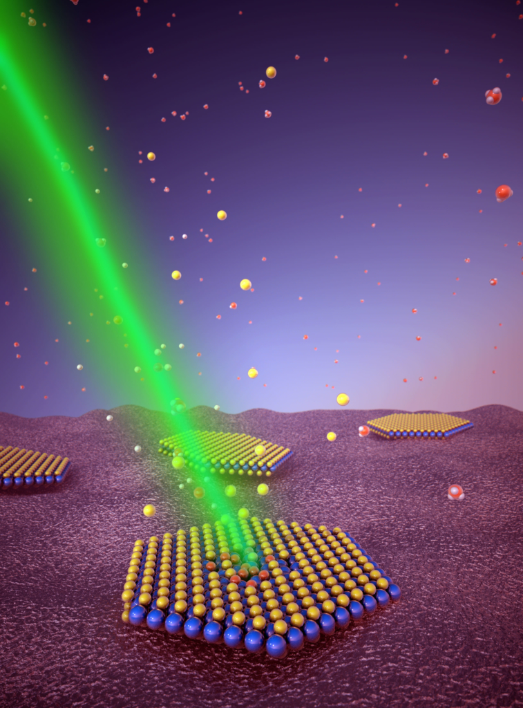
The doping process Grigoropoulos’s group developed involves laser-assisted Chemical Vapor Deposition with standard semiconductor dopant gases and a unique vacuum chamber setup. Multiple lasers operating at different wavelengths are focused onto the sample to provide in-situ control of the spatial distribution and site specific doping levels on TMDCs. The lasers serve two functions: to create vacancies in the TMDC films and simultaneously dissociate dopant gas molecules to be incorporated into the thin films.
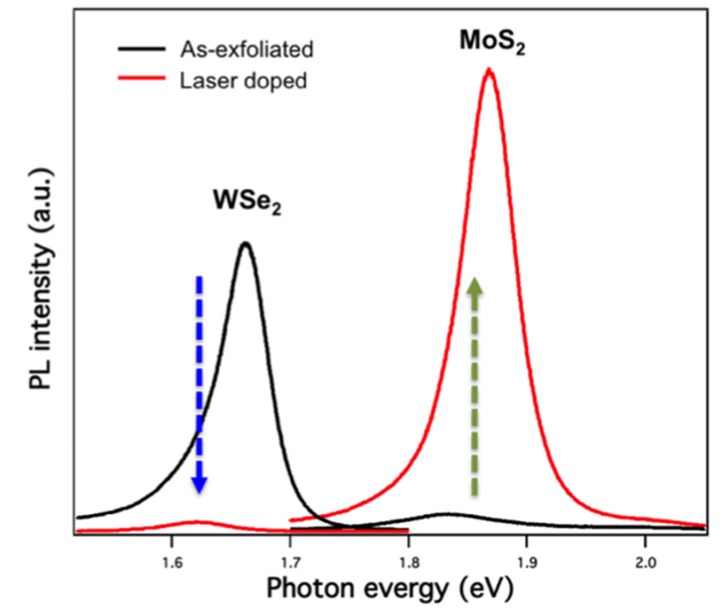
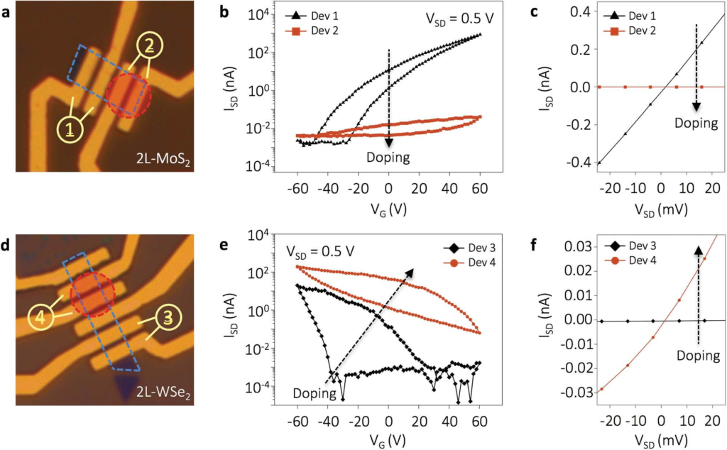
The first part of Grigoropoulos’s group fabricated doped devices from both single and bi-layer flakes of MoS2 and single crystal WS2 and WSe2 materials. They verified the presence of free holes with photoluminescence (PL) characterization experiments and also demonstrated long-term room temperature stability of the doping.
“In contrast with previous attempts on doping TMDCs where device properties would change after a few hours, the doping effect in our process remains undiminished for months, implying incorporation of the dopants into the film structure,” Grigoropoulos says.
“Part of the presentation at ICALEO will additionally show results of our work integrating these devices into flexible platforms. We will present the manufacturing sequence we developed and demonstrate flexible and mechanically robust devices on polymeric substrates,” says Grigoropoulos.
Spatial Benefits
Currently, the group is making junctions and transistors from these doped materials, and working on reducing the beam size even further. Grigoropoulos says this process has the potential to process sub 100 nm or even 20 nm line widths to produce new nano-scale devices that may also unveil new fundamental physics.
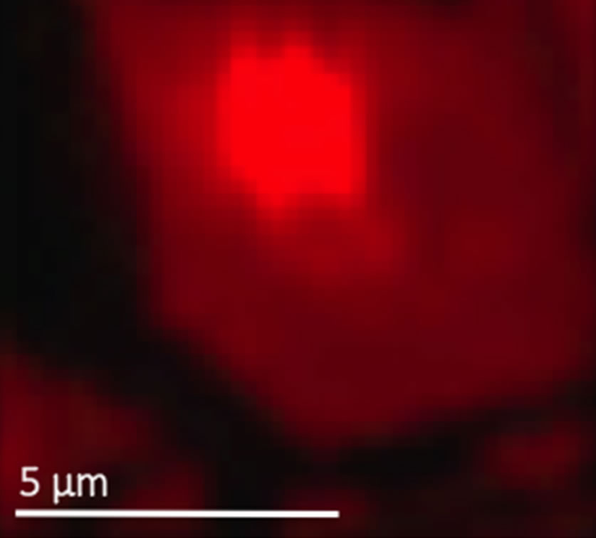
“The main benefit and new feature of laser-based processing is that it is spatially selective. Laser processing tools combined with in-situ imaging allows us to make devices in any arbitrary location. Patterning can be localized to the area desired,” he says.
“TMDCs have been used for tribological purposes because they have low friction. Now, our work improves their functionality and allows them to be doped and used in new ways. By selecting laser wavelength, pulse duration and number of pulses, we can flexibly and precisely tune the target material structure and properties, covering a range of processing parametric space,” he says. “We also have good control of the thermal budget, and avoid damaging the underlying substrate. This is important so the process can be used for polymeric substrates.
“Laser processing is often regarded as a serial process that is perceived as a disadvantage for mass production. But, with nano-scale processing, very low laser power and pulse energies are required. So, using multiple beam arrangements and multi-lens optical configurations can be advantageous and allow scalability to reasonable production levels,” Grigoropoulos says.
Dr. Grigoropoulos will present more on this topic at ICALEO at his invited talk N101 in the Nano1 Session Monday afternoon, October 17, 2016 in San Diego.
Debbie Sniderman is CEO of VI Ventures, an engineering consulting company.