


By Debbie Sniderman
Fabricating through-silicon vias (TSVs) is a key processing technology for 3D silicon IC integration and assembly. These deep holes allow chips to be connected electrically in vertical orientations, completely passing through the entire thickness of silicon wafers, creating 3D ICs for many applications such as image sensors and DRAMS.
Dr. Koji Sugioka’s research team at the RIKEN Center for Advanced Photonics in Japan along with collaborators at the Shanghai Institute Shanghai Institute of Optics and Fine Mechanics in China developed a new laser ablation technology for fabricating high aspect ratio vias using tailored femtosecond Bessel beams.
Maintaining Focus
Bessel beams are non-diffracted beams that don’t spread when they propagate, and remain focused for ranges typically longer than a few millimeters. Sugioka says for forming high aspect ratio features in silicon, using lasers with Bessel beams are advantageous compared to Gaussian beams since it is possible to obtain depths of focus in their axial range much longer than the thickness of typical silicon substrates.
“To generate a Bessel beam inside a material, it must be transparent to it, meaning that the wavelength should be longer than the substrate it is entering,” he explains. “The bandgap of silicon [at 300 K] is 1.12 eV, so to generate a Bessel beam in silicon, a laser with a wavelength longer than 1.1 um must be used. We used a laser with a 1.5 um wavelength.”
“However, true Bessel beams don’t exist in the real world,” says Sugioka. “Current 3D IC technologies require 10:1 aspect ratio (AR) TSVs in 500 um thick Si substrates. In the future, the same AR will be needed on thinner substrates of 50 um. At 50 um thickness, Bessel and Gaussian beams hardly meet the AR requirement, while Bessel beams generate severe sidelobe damage in 10:1 AR tests. But, our idea of tailoring the Bessel beams with a Binary Phase plate (BPP) that acts as a phase filter produced high quality TSVs,” he says.
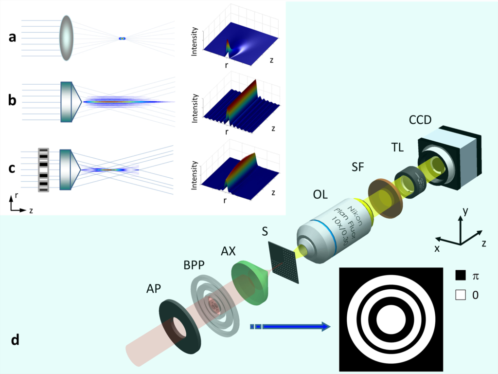
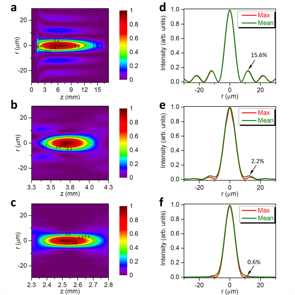
Simulations of the energy profiles within the beams done by collaborators at the Shanghai Institute helped design and fabricate two BPPS. When used in front of the Axicon lens, their concept is to assist delivering sidelobe energy to the center, which also changes the depth of focus. Simulations and tests show they efficiently decrease the sidelobe energy ratio, the ratio of the peak intensity of the maximum sidelobe to that of the central lobe, from 15.6 percent for conventional fs Bessel beams to 0.6 percent.
“They reduce the energy required for TSV fabrication by an order of magnitude compared to using the Axicon lens alone. They also have the unfortunate effect of decreasing the depth of field, but it is responsible for reducing the energy required for TSV fabrication and remains longer than the thickness of the substrate, so they can still be used,” says Sugioka.
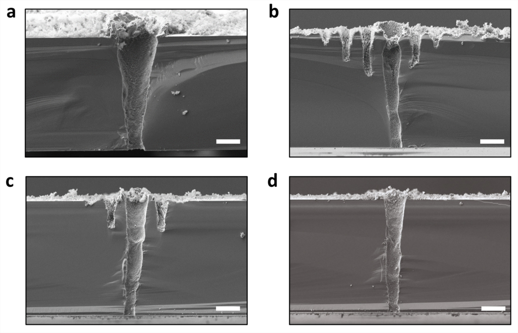
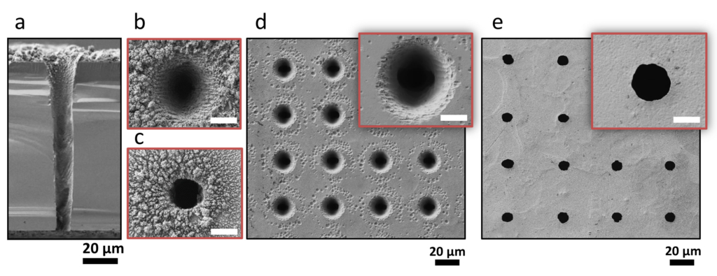
In 50 um substrates, the Figure below shows results of silicon drilling in air and the resulting severely tapered via with AR less than 3 when a Gaussian beam was used in (a). Concentric damage due to the sidelobe is seen in (b) when a conventional Bessel beam only with an Axicon lens was used. Significant improvement is seen in a via with AR larger than 10 in (c) when BPP1 was used, but damage was still present with this specific design. In (d) sidelobe damage has been completely eliminated and a high-aspect-ratio TSV was fabricated using a second BPP design (BPP 2) in front of the Axicon lens.
The next Figure shows that using the combination of BPP2 and the Axicon lens, very high aspect ratio TSVs in 100 um substrates were produced. In contrast, the conventional Bessel beam and the Bessel beam tailored with BPP 1 cannot create TVSs due to multiphoton absorption of sidelobes at the surface.
Real World Advantages
Compared to conventional ways to form TSVs in silicon with Deep Reactive Ion Etching (DRIE), laser processing offers higher etch rates and a reduced number of processing steps since lithography is not needed. No vacuum processing is required, and the laser process is hermetic and more environmentally friendly compared with RIE.
Sugioka says these preliminary results demonstrate proof of concept that TSVs can be produced using a tailored Bessel beam in 100 um thick substrates. Any surface debris present after ablation can be completely removed with acid cleans.
“We can create ‘almost-taper free’ TSVs in 100 um thick substrates with aspect ratios greater than ten, which meets future industrial requirements. We have also demonstrated TSVs with smaller 2-3 um diameters that are not exactly taper-free. Producing completely taper-free TSVs is difficult to do because the energy intensity profile along the beam axis varies, although the beam diameter is constant in this range,” he says. “We’d like to fabricate completely taper-free TSVs, and think that by further optimizing the design of the BPP we can obtain a uniform profile to do so.” Future work is needed to demonstrate the process on 500 um substrates.
“In order to meet industrial requirements the throughput would need to be significantly increased. Our method provides a drilling speed of 1 or 2 vias per pulse, but industry needs 1000-fold faster. We think it can be increased by using a 100 kHz repetition rate laser to 100 holes per second without deteriorating TSV quality, which is still one order of magnitude smaller than needed. We are considering parallel multi-beam processing and combining 100 kHz lasers along with further optimization,” Sugioka says.
Dr. Sugioka will present more on this topic in at ICALEO 2016 in San Diego, at his talk N102 in the Nano1 session Monday afternoon October 17.
Debbie Sniderman is CEO of VI Ventures, an engineering consulting company.