


By: Yung Shin
With the growing need for renewable energy sources, there is an increasing demand for cheap and high-efficiency solar cells. Although high-efficiency silicon solar cells with overall efficiencies higher than 25% [1] have been fabricated in laboratories, the high cost involved in manufacturing these high-efficiency devices makes their commercial use not yet practical. Optical losses through front surface reflections lower the overall efficiency of solar cells since bare silicon reflects nearly 40% of incident solar radiation over the wavelength range of 200 nm to 1100 nm. Anti-reflective coatings have been used to improve solar energy absorption. A more economical alternate solution would be desirable. Texturing the surface of silicon wafers to suppress reflections has been commonly used to improve the efficiency of solar cells [2-5].
Using high-speed, high-power picosecond laser pulse irradiation, low reflectance laser-induced periodic surface structures (LIPSS) could be created on polycrystalline Silicon. A decrease of 35.7% in average reflectance of the silicon wafer was achieved over the wavelength range of 400 nm to 860 nm when it was textured with LIPSS at high scan speeds of 4000 mm/s. A picosecond laser was used to create LIPSS on silicon wafers, which generates linearly polarized pulses with a pulse duration of 10 ps at 532 nm and the focal spot size of 10 µm with a variable repetition rate ranging from 10 KHz to 640 KHz. The period required to achieve the lowest surface reflectance was determined by finite difference time domain (FDTD) simulations, which showed that a period close to 450 nm was the most effective in suppressing reflections in the wavelength range of 200 nm to 1100 nm, which is the range of wavelengths in which silicon solar cells convert light energy to electrical energy. Therefore, the 532 nm wavelength of the laser was chosen with the repetition rate of 640 KHz and a scan speed of 4000 mm/s to create uniform LIPSS over an area of 4 cm by 4 cm. A computer-controlled precision 3-axis stage was used to position the silicon sample under the scanner head. The silicon samples used are 127 mm diameter, 525 µm thick polished wafers. The silicon is N doped with phosphorous and its crystal orientation is (111) with the electrical resistivity less than 0.006 ohm-cm. In order to create LIPSS, the laser was scanned over the surface of the wafer, which was positioned at the focal length of the objective lens. All experiments were conducted with ambient air as the irradiation atmosphere.
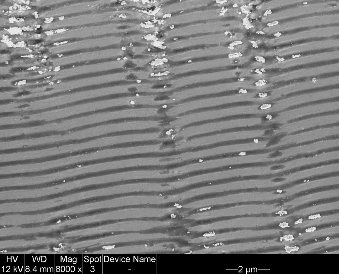
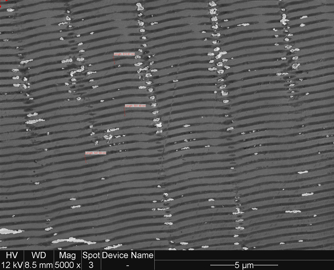
SEM images revealed that the LIPSS had a period of 532 nm and a fill factor of 75%. The depth of the channels was found to increase with increasing fluence. At 0.8 J/cm2, highly uniform structures were obtained with no surface material removal. The periodic structures appeared to have a flat top surface with filleted edges and deep, narrow valleys. The depth of the valleys was determined through atomic force microscope imaging and was found to range from 150 nm to 350 nm. Fig. 1 shows SEM images of the highly periodic LIPSS created at a fluence of 0.8 J/cm2. At higher fluence values up to 1 J/cm2, the valley depth was found to increase and light was trapped more effectively. At a fluence of 1.1 J/cm2, deep and continuous LIPSS were formed, resulting in an average reflectance of 23.1% corresponding to a 35.7% decrease in average reflectance compared to bare silicon. At even higher fluence values up to 1.2 J/cm2, deep valleys were created with irregularities due to material removal. This resulted in even lower reflectance values due to increased scattering of light below the surface of the material. Beyond this fluence value, the structures no longer appeared periodic. Deep craters and surface irregularities were formed which further enhanced scattering and light trapping below the surface, thus decreasing the average reflectance. Fig. 2 shows the reflectance curves for structures created at different fluence values, across the wavelength range of 400 nm to 860 nm. A clear decreasing trend in reflectance is seen as the fluence is increased. Above this fluence, material removal causes severe damage to the surface.

In order to measure the broadband reflectance of the sample, a Perklin Elmer spectrophotometer was used. First, the sample was checked for opacity, and then the spectral reflectance (R) and transmittance (T) were measured over the wavelength range of 200 nm to 1200 nm. A monochromator was used to resolve the wavelength. Structures made with increasing fluence values exhibited a trend of decreasing average reflectance value. As the fluence was increased from 0.95 J/cm2 to 1.4 J/cm2, the average reflectance over the wavelength range of 400 nm to 860 nm decreased from 25.79% to 19.84%. Fig. 2 shows the reflectance curves for structures created at different fluence values, across the wavelength range of 400 nm to 860 nm. As compared to the reflectance of bare silicon which was measured to be 35.93% over the same wavelength range, a 44.8% decrease in reflectance was achieved for the case of texturing at 1.4 J/cm2. This drop is attributed to the increasing depth of channels and increasing irregularities on the surface.
In summary, silicon wafers with average reflectance values of 23.1% were fabricated by texturing the surface with a picosecond laser. These structures were created at high laser scanning speeds of 4000 mm/s and low pulse overlapping ratios of 60%. Picosecond lasers, due to their lower power density, high rep. rate, and high pulse energy, were shown to be ideal for high-speed surface texturing. With the availability of high-power, high-repetition picosecond laser, the processing speed can further increase, offering the possibility of surface texturing during roll-to-roll manufacturing processes. This method provides an inexpensive and rapid process to create low-reflectance silicon wafers which can be used in photovoltaic applications.
Yung C. Shin is a professor and director at the Center for Laser-based Manufacturing for the School of Mechanical Engineering at Purdue University.
References:
1.) M. A. Green, K. Emery, Y. Hishikawa, W. Warta and E. D. Dunlop, Solar cell efficiency tables (Version 45), Prog. Photovolt: Res. Appl. 2015, 23:1–9
2.) J. I. Gittleman, E. K. Sichel, H. W. Lehmann, and R. Widmer, Textured silicon: A selective absorber for solar thermal conversion, Appl. Phys. Lett. 35, 742 (1979), http://dx.doi.org/10.1063/1.90953
3.) A.W. Smith and A. Rohatgi, A new texturing geometry for producing high efficiency solar cells with no antireflection coatings, Sol. Energ. Mat. Sol. Cells 29 (1993) 51-65
4.)S. Winderbaum, O. Reinhold, F. Yun, Reactive ion etching (RIE) as a method for texturing polycrystalline silicon solar cells, Sol. Energ. Mat. Sol. Cells 46 (1997) 239-248
5.) D.H. Macdonald, A. Cuevas, M.J. Kerr, C. Samundsett, D. Ruby, S. Winderbaum, A. Leo, Texturing industrial multicrystalline silicon solar cells, Sol. Energ. 76 (2004) 277–283