As featured in the LIA TODAY
By Liliana Caldero
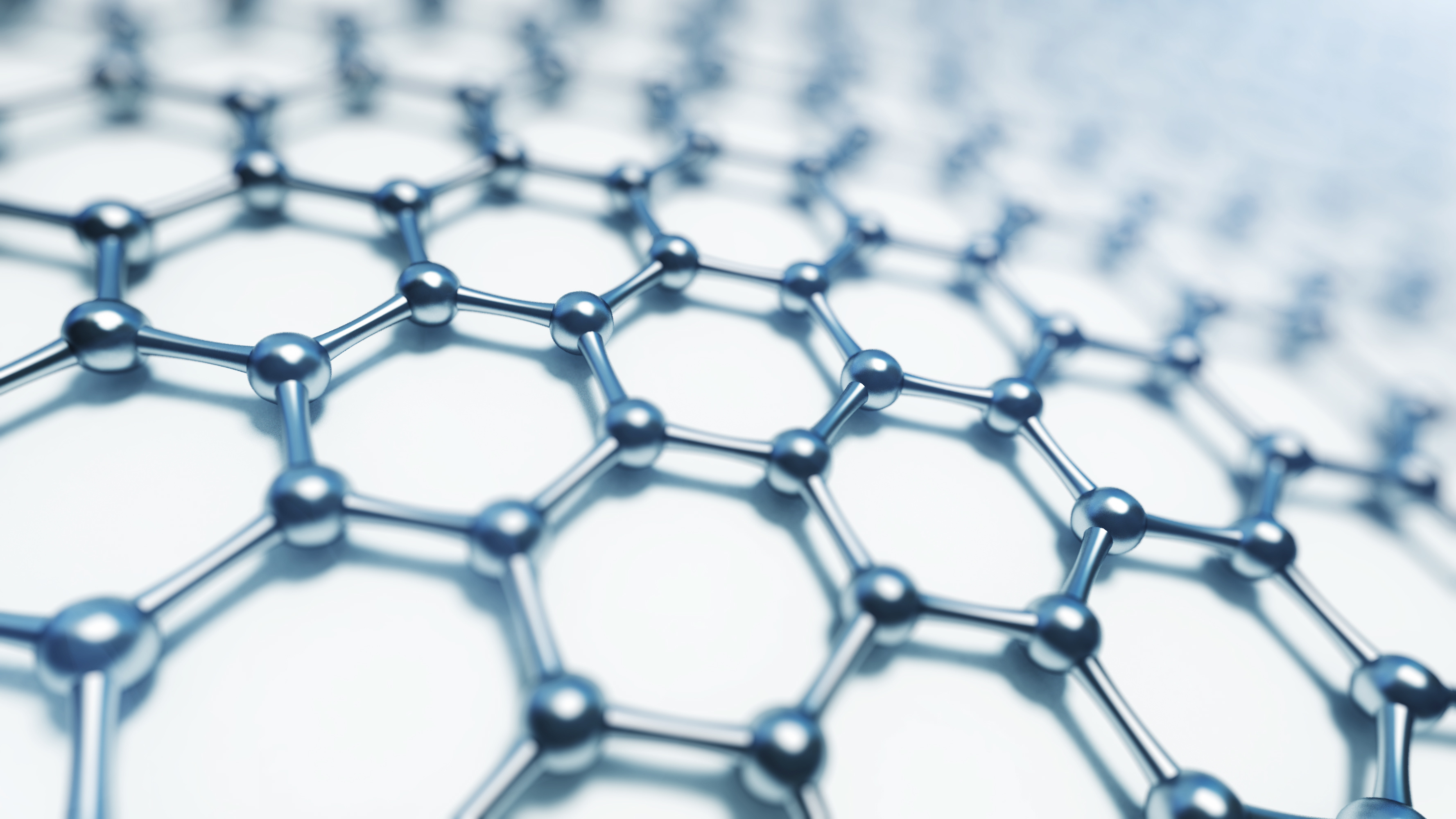
Graphene – it’s the two-dimensional (2D) allotrope of carbon atoms that ignited the imaginations of researchers across the globe. Heralded as a ‘miracle material’, its potential seemed limitless and it was predicted to usher in the next generation of technology. Flexible, stronger than steel, transparent, lightweight, and an amazing conductor of heat and electricity, it was going to revolutionize everything from household electronics to biomedical nanotechnology.
THE PROBLEM
Yet, nearly eight years after Dr. Andre Geim and Dr. Konstantin Novoselov earned the Nobel Prize in Physics for first isolating graphene and identifying its properties, graphene has encountered barriers to moving out of the lab and into the marketplace. According to Prof. Dr. Aravinda Kar of the University of Central Florida’s Center for Research and Education in Optics and Lasers (CREOL), one of the most prominent barriers has been finding scalable manufacturing processes that can produce graphene of a quality and quantity ready for consumers and businesses.
Graphene is notoriously difficult to synthesize in large quantities at a consistent quality. Early methods of isolating graphene involved a slow and tedious mechanical exfoliation technique; the researchers would extract a thin layer of graphite from a graphite crystal using regular adhesive tape, continually reducing the graphite sample by sticking the tape together and pulling it apart until only a small, 2D section of carbon atoms with a honeycomb lattice remained. Graphene’s unique characteristics are only present when it is one, two, or three layers of atoms thick – any thicker and it becomes graphite, losing all of the exceptional properties of graphene. The tape exfoliation method, although useful for the lab, was not going to translate very well to an industrialized process.
SOLVENT-AIDED EXFOLIATION AND CVD
Two of the more promising and potentially scalable methods of producing graphene are solvent-aided exfoliation and chemical vapor deposition (CVD). In solvent-aided exfoliation, sonication is used to exfoliate graphene crystals which are then further separated in a solvent and later gathered into graphene monolayers. Scientists at the National University of Singapore have identified a flocculation method that reduces the amount of solvent needed for their exfoliation process, which could yield graphene using far less solvent than was previously needed. Another method experiencing innovation is CVD, which uses thermal chemical reactions to ‘grow’ graphene on substrates of specific materials, typically copper or silicon. Recently, engineers at MIT developed a CVD process for producing graphene filtration membrane sheets at 5 cm per minute. One of the biggest issues with traditional CVD and exfoliation methods is the need to transfer graphene from its fabrication platform to a substrate. Lasers are going to change that.
THE MISSING PIECE – LASERS
Lasers may provide yet another avenue to the elusive mass production of graphene, with an eye toward innovating the semiconductor industry. In 2003, Kar, along with Dr. Islam Salama and Dr. Nathaniel Quick, realized that laser direct writing could be used to fabricate carbon-rich nanoribbons on a silicon carbide (SiC) wafer in a nitrogen rich environment. Although these ribbons were too thick to be considered graphene, Kar believed that with a few changes, this process could be reworked to synthesize graphene in situ on a large scale, very quickly. In 2013, Kar and Quick were issued a patent for a Laser Chemical Vapor Deposition (LCVD) method that could be scaled for mass production.
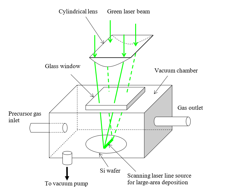
Their method involved a few simple components: a frequency doubled Nd:YAG (green) laser of 532 nm wavelength, methane (CH4) gas, a silicon substrate, and a vacuum chamber.
The 532 nm wavelength corresponds to a photon of energy 2.33 eV, so the energy of two photons is 4.66 eV, just within the range of the C-H bond energy (4.3-4.85 eV) in CH4. Focusing the laser beam to a high intensity can induce two-photon absorption at the focal plane, causing the decomposition of CH4 to release the hydrogen atoms and deposit carbon atoms only on the substrate. The laser heating of the silicon substrate is just low enough to avoid melting the silicon, while providing sufficient thermal and electromagnetic energies to assist the carbon-carbon bonds rearrange into graphene’s trademark hexagonal pattern.

LASER DIRECT WRITING OF GRAPHENE
Kar believes this process could be adapted to add graphene directly onto any substrate. Using laser direct writing, a company could easily draw graphene circuits onto a board. For companies using a hybrid approach, the graphene could be deposited at precise points as interconnects. “You would have all the CAD/CAM capability you could want,” says Quick. Currently, green lasers are available at high output powers, 100 W in continuous wave mode from most large laser manufacturers, so adding this additional step to the manufacturing pipeline for semiconductors would be easy and inexpensive compared to other methods.
At 1.9 cm per second, or 45 inches per minute, this method of graphene production is fast and efficient. This LCVD method offers control over the number of graphene layers, whether one, two, or three are required. This process also removes the need to manually place graphene onto its intended location, as it is synthesized precisely where it should be. It’s also worth mentioning that this process is conducive to minimal environmental impact, as the unreacted methane and hydrogen byproducts can be captured to be recycled and reused.
A LOOK AT THE FUTURE
Picture this: a template is placed over a substrate and a line-shaped laser beam sweeps over it briefly or a beam of large cross-sectional area illuminates the entire template in one shot; when the template is removed, an intricate graphene design has been printed onto a circuit board. That is the future that Kar says is possible, with the right equipment. He suggests that we need manufacturers to develop lasers producing line-shaped beams or large area beams with spatially uniform intensity profile to realize this vision cost-effectively. He emphasizes that a true line-shaped beam produced by a slab laser system or an array of optical fiber laser would be necessary, as shaping the beam synthetically by changing the shape of an aperture would result in too much lost energy. With this technology, graphene could easily be printed onto circuit boards immediately, only where it’s needed, saving in material costs and time.
Nearly 14 years after the excitement first began, researchers are still exploring the potential uses of graphene; from applications in microsupercapacitors to Organic LEDs in flexible displays to ultra-sensitive optical sensors, and even lightweight body armor, the possibilities are still as exciting as ever.
Acknowledgements
Prof. Dr. Aravinda Kar, University of Central Florida, CREOL
Dr. Nathaniel Quick, Executive Director of LIA
LEARN MORE
Laser Formation of Graphene: United States Patent 8617669. (N. Quick, A. Kar)
http://www.freepatentsonline.com/8617669.html
NUS-led research team develops cost effective technique for mass production of high-quality graphene – http://news.nus.edu.sg/press-releases/mass-production-graphene-slurry
MIT researchers develop scalable manufacturing process for graphene sheets – https://newatlas.com/mit-manufacturing-graphene-filtration-membranes/54274/


