As featured in the LIA TODAY and ICALEO 2017
By Jinguang Cai and Akira Watanabe
The development of miniaturized portable and wearable electronic devices has attracted worldwide research attention, due to their increasing integration with human daily life. Different from traditional electronic devices on “hard” boards, such devices should be soft and flexible. A concept called “flexible hybrid electronics”, which is a hybrid of soft and hard parts, has been proposed to address the fabrication issue of flexible devices.

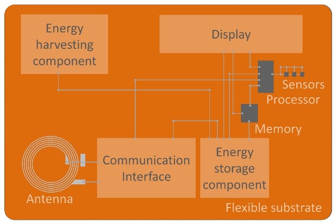
The concept of a flexible hybrid electronic device is illustrated in Fig.1, in which “soft parts”, such as electronic interconnection, energy harvesting and energy storage components, antennae, and even displays, sensors, and communication interfaces, can be prepared via printing methods. “hard parts”, such as processor and memory, can be provided by the commercial small-size silicon components, which are small enough, and can be integrated into the device without influencing the flexibility. However, printing methods have some issues such as limitation of materials, high cost of inks, and complicated post-processing.
Laser direct writing is a non-contact, fast single-step fabrication technique without requirements for masks, post-processing, and complex clean environments. Meanwhile, various kinds of lasers have been rapidly developed with relatively low costs and broad available wavelengths and powers, and widely used in industry for materials welding, cutting, and polishing. Besides, laser processing can be focused into a micrometer-sized or submicrometer-sized area to realize on-demand fabrication of functional micro-patterns, showing the potential to be integrated into current product lines for commercial use. Laser direct writing has been demonstrated to prepare energy harvesting and energy storage components, electronic circuits, sensors, communication interface, and antennae.
Energy harvesting and storage components
Generally, a flexible device employs a thin film battery as the energy storage and supply unit, in combination with a flexible energy harvesting device such as a polymer solar cell. Recently, as a new type of energy storage device, micro-supercapacitors (MSCs), has been developed and recognized as potential power supply units for on-chip micro-devices, because they possess not only the advantages of supercapacitors such as high power density, excellent cycling stability, pollution-free operation, maintenance-free feature, and flexibility, but also simplified packaging processes and compatibility with integrated circuits. Among various materials for supercapacitors, carbon materials possess the properties which can satisfy the requirements of MSCs in the flexible devices, such as high specific surface area, high electrical conductivity, high electrochemical stability, and high mechanical tolerance.

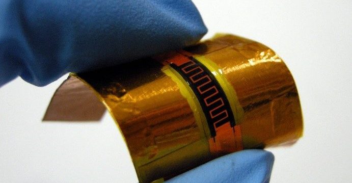
Laser-induced carbonization of polymers such as polyimide has been demonstrated to prepare flexible all-solid-state carbon-based MSCs with high performance by laser direct writing on a polyimide (PI) film in air (Fig. 2). In order to suppress the oxidation process and thus, increase the conductivity of the laser-induced carbon structures, the laser direct writing was conducted on PI films in an inert gas such as Ar, resulting in carbon MSCs with improved volumetric energy density and power density. Furthermore, high-conductive Au nanoparticles can be incorporated to construct double-layer carbon/Au composite electrodes with improved conductivity by two-step laser direct writing.
It will be beneficial for practical use if energy harvest and storage units can be integrated into the same device. As a demonstration, TiO2 nanoparticles were deposited on one side of the laser-written interdigitated carbon electrodes by an electrophoretic method, forming carbon/TiO2 composite MSC with photo-rechargeable capability under UV irradiation due to the photovoltaic property of TiO2 nanoparticles. Although the charging voltage is not high enough for practical use currently, it is expected that such a strategy can be developed for practical use by optimizing the photo-absorption materials and the combination.

Photodetectors and humidity sensors
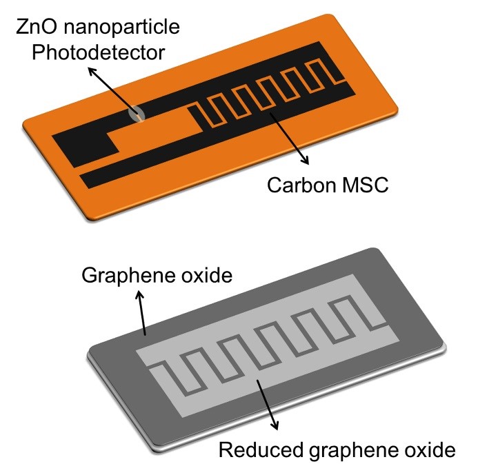
Sensors are one of the most important interfaces with users in IoT (Internet of Things) technology, thence it is very important to develop various types of sensors for flexible devices. Laser direct writing can play an important role in preparing sensors directly on the flexible substrate with high performance and stability. For example, a photodetector for UV light can be fabricated by laser direct writing and deposition of ZnO nanoparticles, and can be integrated into the PI film with a carbon MSC fabricated by laser-induced carbonization, forming an integrated photodetector for practical use (Fig. 3, Top). Besides, a humidity sensor based on an interdigitated reduced graphene oxide (rGO)/graphene oxide (GO)/rGO structure prepared by laser direct writing was also demonstrated with high and fast response, flexibility, and long-term stability, showing the potential to be used in flexible devices (Fig. 3, Bottom).

Circuits, communication interface, and antenna
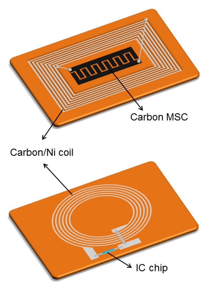
High-conductive metallic circuits with mechanical stability are very important in flexible devices as basic structures, and their preparation should be facile, cost-effective, and easily integrated with other electronic components. Laser direct writing has been demonstrated to pattern metallic Pd on PI films, which can act as catalysts in the electroless Ni plating process, producing high-conductive carbon/Ni composite structures. The carbon/Ni structures exhibited a certain flexibility and excellent anti-scratch performance due to the intimate deposition of Ni layer on carbon surfaces. Such carbon/Ni structures can be used as conductive circuits to construct practical devices. For example, a wireless charging and storage device can be fabricated by integrating an outer rectangle carbon/Ni composite coil for harvesting electromagnetic waves and an inner carbon MSC for energy storage, which can be fast charged by a commercial wireless charger (Fig. 4, Top). In addition, a near-field communication (NFC) antenna was prepared using a carbon/Ni composite coil, and acted as a communication interface with an NFC smartphone for harvesting signals, and an ultra-small commercial IC chip was integrated for data storage (Fig. 4, Bottom). The integrated NFC tag can be used for practical application.
Summary & outlook
While laser direct writing has been demonstrated to be an effective approach to preparing most of the components in flexible devices, such as carbon MSCs as energy storage unit, carbon/TiO2 MSCs for energy harvesting and storage unit, photodetectors and humidity sensors, high-conductive carbon/Ni structures for electronic circuits, and even integrated wireless devices, many efforts are still required to promote the laser direct writing technique applied in the development of flexible hybrid electronics for practical applications in IoT in the future.
Jinguang Cai, Institute of Materials, China Academy of Engineering Physics, Jiangyou 621908, Sichuan, P. R. China
Akira Watanabe, Institute of Multidisciplinary Research for Advanced Materials, Tohoku University, 2-1-1 Katahira, Aoba-ku, Sendai 980-8577, Japan


