High Growth Areas in Industrial Laser Processing & Monitoring

By Craig Bratt & Rahul Patwa

The brilliant light of the laser promises unlimited possibilities for materials processing. Its use in manufacturing dates back to the late 1960s where laser drilling was developed for jet engine components. As laser technology has progressed, fast-paced advances in computers and sensor technologies have enabled the development of improved process monitoring devices which has further enhanced the performance, reliability and ease of use of industrial laser systems.

In 2014, the total global market for laser systems for material processing which include both the source and the components was $9.2 Billion (Source: Optech Consulting, VDMA). From this, the total global laser source revenue was $2.9 Billion, according to the data presented by Industrial Laser Solutions (Feb 2016). In 2015, this revenue (only the global laser source revenue) increased by 6.9% to $3.2 Billion. Although, the largest market share has been and continues to be (61% in 2015) in the laser cutting and laser marking/engraving, their % year-over-year growth has been limited to <5%. More interestingly, the higher % Y-O-Y growth areas are laser welding (17%), laser surface treatment (31%) and laser additive manufacturing (71%).

Courtesy Image

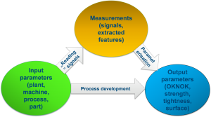
In this article, we present a clear view of how advances in laser power and beam quality along with a significant drop in laser cost per watt and improved laser wall plug efficiency has contributed to major innovations in laser material processing. We have identified four broad laser processing segments and analyzed what is driving innovation.

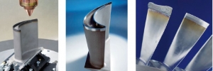
Manufacturers in many industries have long used laser welding to tackle traditional welding challenges, but laser welding technologies are evolving for even greater utility. Hybrid welding where laser welding is combined with other conventional arc welding methods such as GMAW (MIG) and GTAW (TIG), laser welding with filler wire, and part pre-heating have been successfully implemented in Industry. This has been possible now due to the availability of higher power lasers at lower cost. In turn, materials that were considered difficult to weld until now such as higher carbon steels and cast iron can now be successfully laser welded. The additional filler material changes the composition of the weld, preventing the formation of hard and brittle microstructures. Likewise, induction preheating can be used to help prevent cracking due to martensite formation by slowing down the cooling rate after welding. For instance, in an automotive transmission part, a bolting process was replaced with laser welding, cost savings were achieved through reduced material and processing costs (drilling operations / bolting operations and the bolts themselves), and an overall part weight reduction was accomplished with a more efficient production method using laser technology.

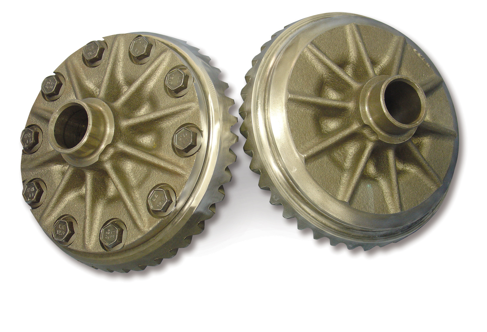
Laser welded transmission part versus traditionally bolted assembly (Courtesy image)

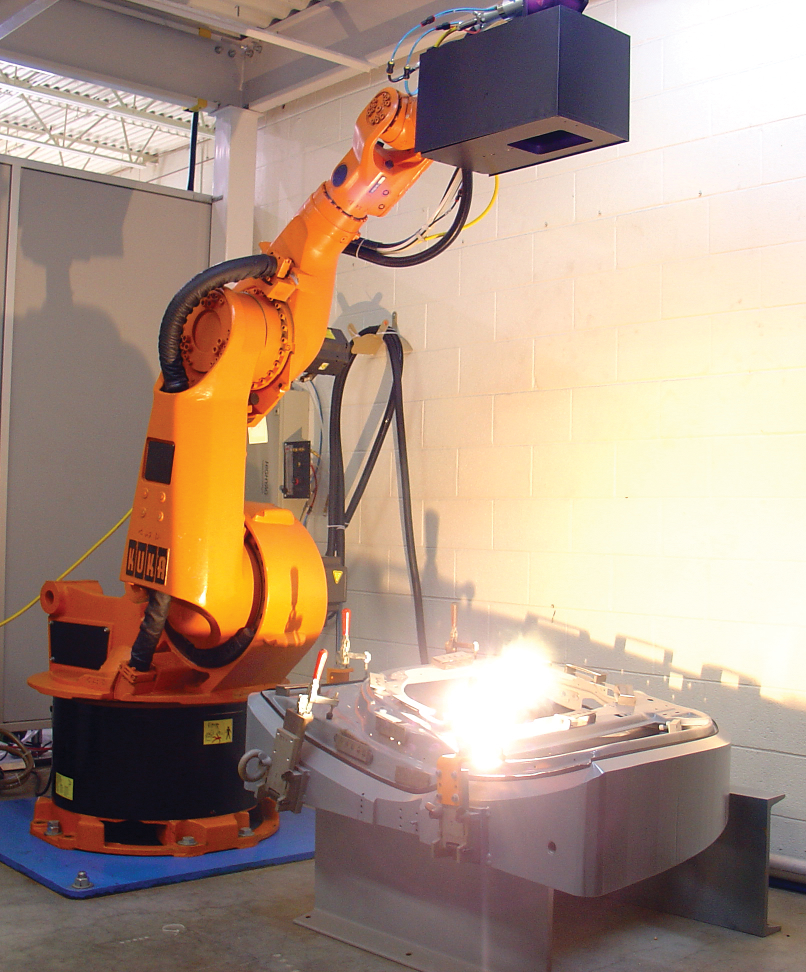
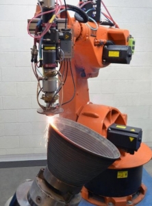
Laser remote welding(Courtesy image)

Remote laser welding is another laser welding process which dramatically reduces welding process cycle times compared to conventional welding and is now possible due to availability of higher beam quality lasers and high speed scanners. It involves the use of moving optics in order to rapidly scan the laser beam across the workpiece over large distances both for high speed and for high precision point to point movement.

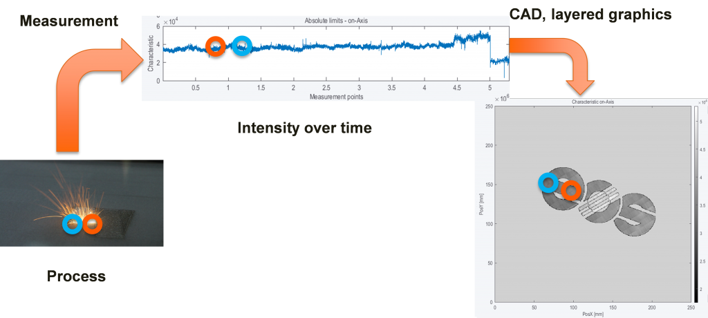
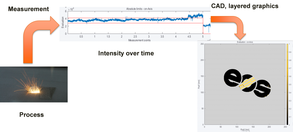
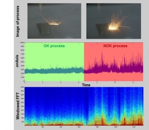
To capture the higher potential of laser welding, there has been substantial yet continuous development in laser welding head technology which includes the welding optics themselves and also the sensor optics. Some of these process monitoring technologies have been in development for some time. Some are not yet ready for application at scale. But camera based laser monitoring is now at a point where its greater reliability and lower cost is starting to make sense for high power welding applications.

Fraunhofer CLA has developed a high speed camera vision system which can record the welding process in high clarity in real-time and provide both image and video data from the process. This information is processed and calibrated with reference data based on pre-determined actual ‘good’ weld measurements using reinforcement learning. Using customized image processing software algorithms, it is possible to detect many of the most common weld defects.

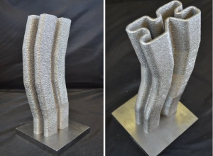
One laser processing technology which has recently been moving up to forefront of innovative, or even disruptive technologies is laser additive manufacturing (LAM). This process uses laser beam as heat source and is primarily divided in two processes: Selective laser melting (SLM) and Laser metal deposition (LMD).

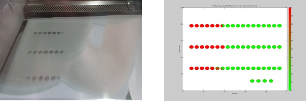
In the SLM process, a layer of powder is deposited on a build platform and then a rapidly scanned laser beam fuses powder together in the right shape and multiple thin powder layers are deposited to create complex 3D parts.

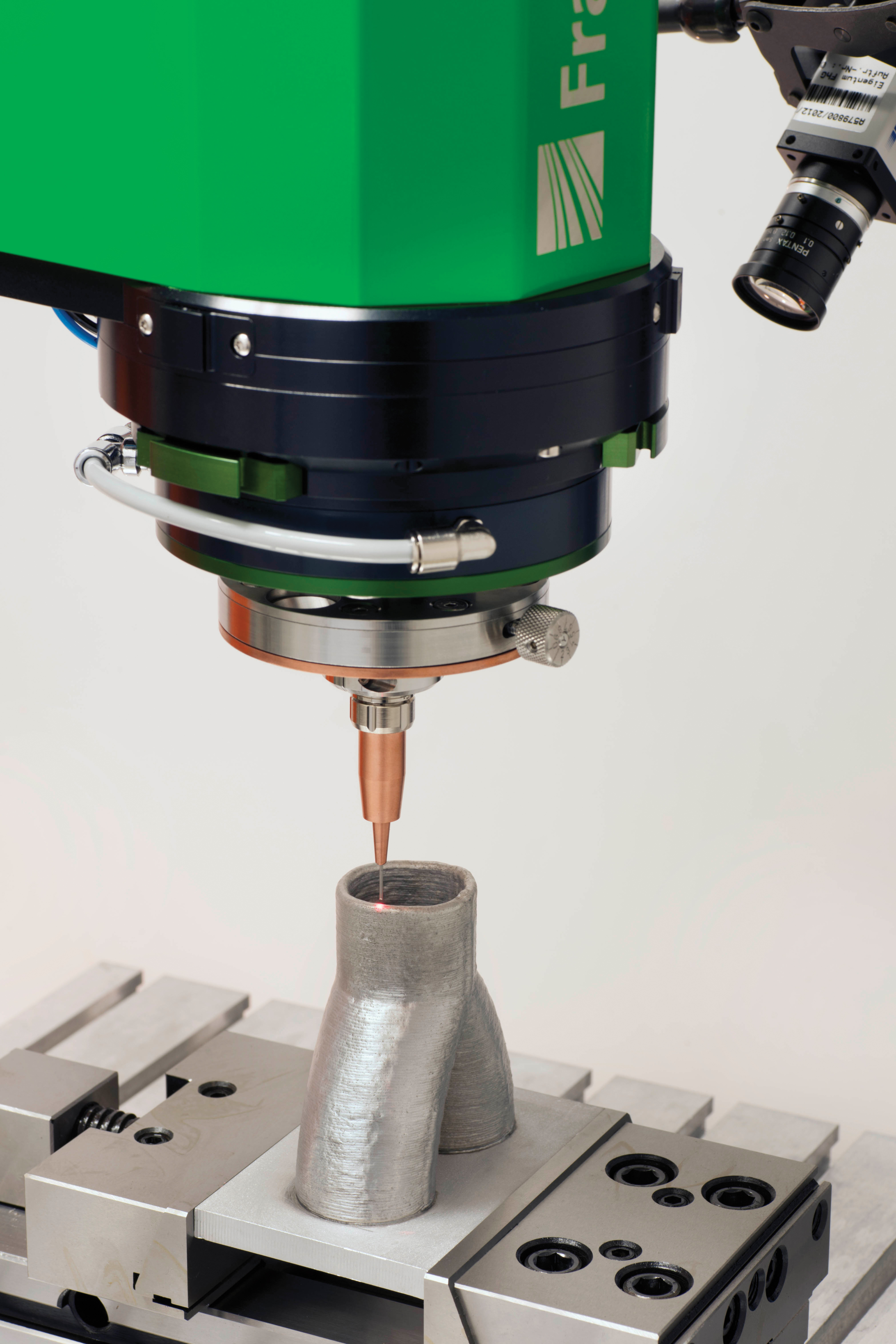
Fraunhofer Coax wire deposition head allows multi directional build up using wire. (Courtesy image)

In the LMD process (also known as direct energy deposition or laser cladding), the laser is used to melt metal powder fed through the nozzle which is then deposited in layers onto a substrate, which results in a full metallurgical bond with a small heat affected zone and minimal dilution. It has been developed for surface wear and corrosion coatings, component repairs/remanufacturing, and generation of complete components from scratch.

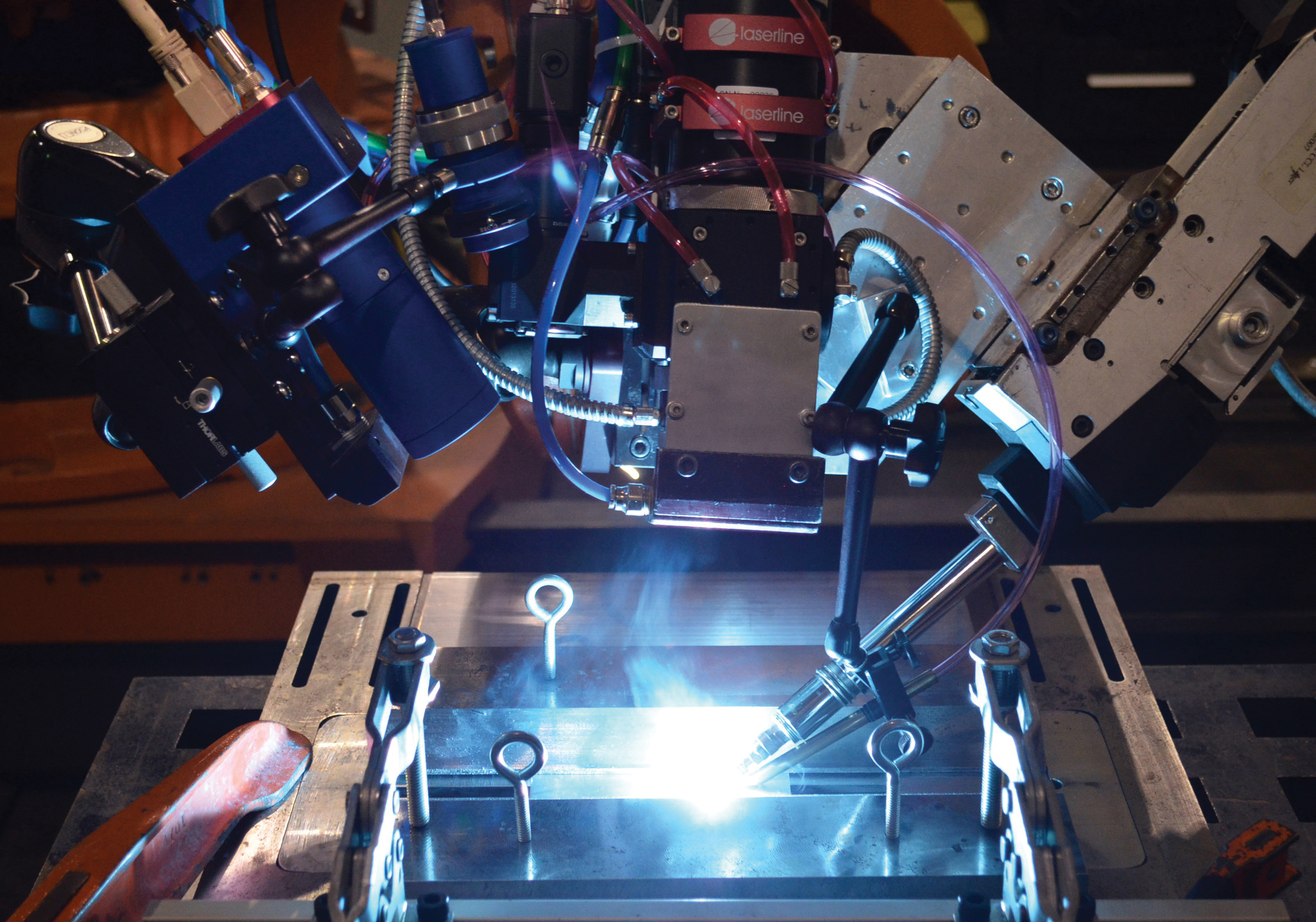
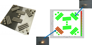
Fraunhofer process monitoring system hardware (Courtesy image)

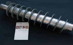
Two other variations of LMD—hot/cold wire cladding and internal diameter cladding—have now evolved into successful industrial processes and are now widely used in the oil industry, agriculture, power generation and remanufacturing sectors. A recent key development by Fraunhofer IWS is a new coax laser deposition head COAXwireTM which provides
omni-directional welding performance for the use of metallic wires as filler material which is of particular use for 3D build up additive manufacturing of metallic components.

One area of laser material processing that has benefitted the most from technology improvements in both spatial and temporal properties of the laser is laser machining. In addition, the advent of lower cost and smaller footprint laser power sources has lead to much wider industrial adoption of laser technology. The latest generation of pulsed lasers with pulse lengths—from millisecond all the way to femtosecond—has led to a rich pipeline of innovations impacting virtually every manufacturing industry. For example, laser cutting of battery electrodes can produce excellent cut quality and achieve high cutting speeds for application in lithium-ion battery cell production. Similarly lasers can be used for coating removal for electrical contacts on battery foils. Large area coating removal for paint stripping, deoxidization, mold and die cleaning or removal of special coatings is conducted by applying high power lasers. Lasers are also used for high rate drilling process for up to 15,000 holes/second.

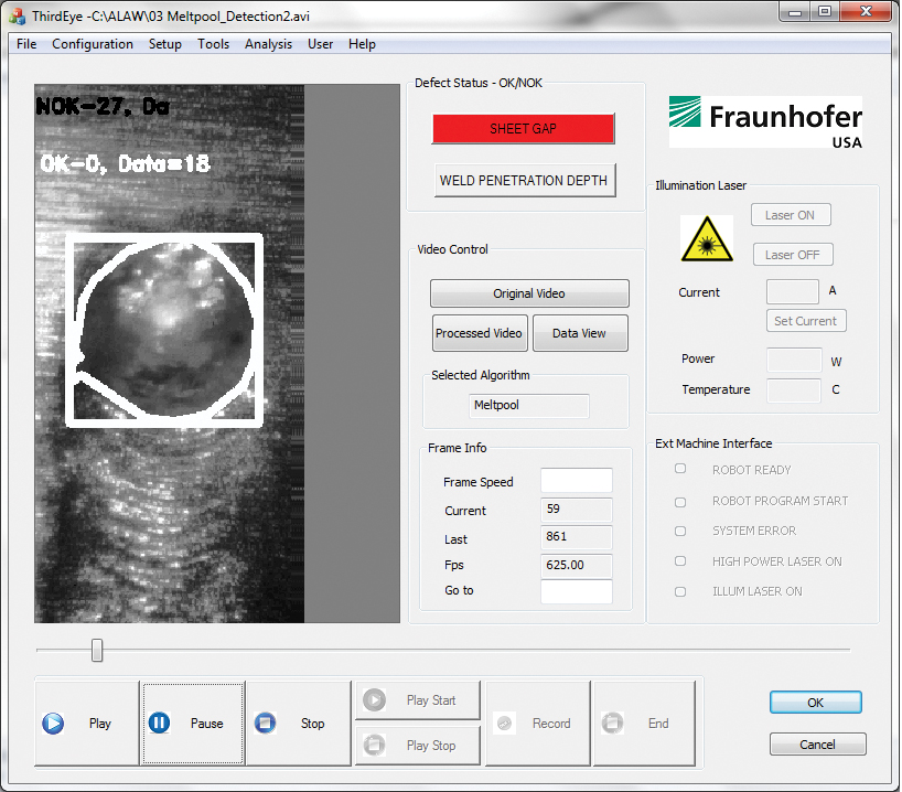
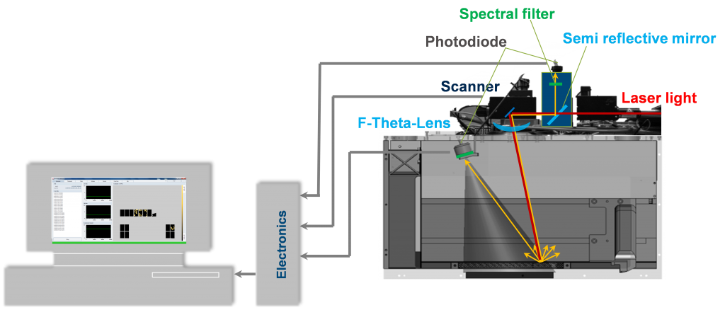
Fraunhofer high speed camera system software (Courtesy image)

In summary, the current pace of innovations leading to new laser technologies and products is constantly increasing with a wide array of new applications being developed for every industry imaginable.

Craig Bratt, Executive Director, Fraunhofer USA, Center for Laser Applications, cbratt@fraunhofer.org

Rahul Patwa, Project Manager, Fraunhofer USA, Center for Laser Applications, rpatwa@fraunhofer.org

LIA Presents Professor Reinhart Poprawe with Peter M. Baker Leadership Award

Laser Institute of America presented Professor Reinhart Poprawe, managing director of Fraunhofer Institute for Laser Technology (ILT), the Peter M. Baker Leadership Award during this year’s International Congress on Applications of Lasers & Electro-Optics (ICALEO®) in Atlanta, Georgia, Oct. 22-26.

Lin Li (right), former LIA president, presented LIA’s Peter M. Baker Leadership Award to Professor Reinhart Poprawe(left), at ICALEO, Oct. 25 in Atlanta, Georgia.

The award acknowledges individuals who demonstrate outstanding leadership in an organization while significantly benefiting the laser community.  It is named after former LIA executive director, Peter M. Baker, who led LIA for almost three decades.

“There is no question that Professor Poprawe richly deserves this award. In our world of lasers, he is a leader on the grand scale, technical, organizational, political and social,” Baker said. “He is a fine gentleman, courteous, thoughtful, generous and funny. I consider it an honor to be his friend.”

Poprawe’s professional expertise includes laser applications, laser additive manufacturing, and photonics in life science. Additionally, he has a great deal of experience in laser development and plasma technology in the realms of process analysis, sensors for laser processes, laser induced plasmas and more.

“The award is from one of the most important laser communities in the world,” Poprawe said. “It is a great honor to receive this award as the first recipient after the original, Mr. Peter Baker himself.”

According to several of his peers, Poprawe has been an important figure within the industry for decades.

Professor Reinhart Poprawe addresses a crowd at ICALEO, Oct. 25 in Atlanta, Georgia.

“Professor Poprawe has been an important figure here at LIA for years,” said Nat Quick, LIA’s executive director. “He has been an LIA board member since 2001 and he always steps up when it counts most. He served as an LIA president in 2012 and has functioned as editor-in-chief of the Journal of Laser Applications® (JLA) since 2010. He is incredibly generous and exemplifies what it means to be a leader.”

After earning his Physics Ph.D. in Germany, Poprawe worked as the laser-oriented process development department head for Fraunhofer ILT before becoming their managing director. Additionally, he holds the university chair for Laser Technology at the RWTH Aachen University.

“There are so many ingredients for a successful organization,” Poprawe said. “Vision; mission; research and product portfolios; roadmaps; SWOT-analysis; and education of the employees. Industry or even better societal use and implementation of our research results is what we do everything for, especially the development of the demanding competencies in the very fundamentals of Laser Technology and application Physics.”


About LIA

The Laser Institute of America (LIA) is the professional society for laser applications and safety serving the industrial, educational, medical, research and government communities throughout the world since 1968. www.lia.org, 13501 Ingenuity Drive, Suite 128, Orlando, FL 32826, +1.407.380.1553.


Laser Institute of America Presents Additive Manufacturing: Trends in North America Session at World of Photonics Congress 2017

As part of the World of Photonics Congress’s Additive Manufacturing subconference at LiM 2017, North American laser manufacturing leaders shared a comprehensive look at the latest developments and innovations.

ORLANDO, FL – The Laser Institute of America (LIA) presented its 90 minute session,  AM: Trends in North America, on Wednesday, June 28, 2017 at the International Congress Center in Munich, Germany. The session was part of the Additive Manufacturing subconference of Lasers in Manufacturing (LiM) 2017 at the World of Photonics Congress Lasers in Manufacturing event, held from June 26-29, 2017 and organized by the German Scientific Laser Society (WLT).

The session was part of the Additive Manufacturing subconference of Lasers in Manufacturing (LiM) 2017 at the World of Photonics Congress Lasers in Manufacturing event.

Lasers in Manufacturing (LiM) is a scientific conference focusing on the latest trends in laser materials processing for industrial applications. LiM prides itself as a comprehensive international forum for researchers and experts in laser-based manufacturing.

World of Photonics Congress meets biannually, uniting the “scientific elite” to gather information in the realm of photonics research. The event covers all aspects of research from application-based topics, to the latest applications in industry and medicine. World of Photonics Congress also offers conferences and practice-oriented application panels.

LIA shares in the World of Photonics Congress’s mission of providing laser professionals with valuable events that present and discuss innovative insights with the laser community. The new 90-minute session specifically focused on North American additive manufacturing bolstered the body of knowledge in industry research at the global LiM gathering.

“LIA was honored to collaborate with World of Photonics Congress on this year’s inaugural North American additive manufacturing event,” said Jim Naugle, LIA’s Marketing Director. “We are excited to add our insight and knowledge to the collective expertise found at LiM and are thrilled about this year’s robust attendance. Due to its success, we look forward to possibly expanding our role at future events.”

Attendees enjoyed the unique perspective on the success of North American AM regarding cost and increased efficiency. Keynote speaker David Ott of the Global Humanitarian Lab (GHL)

Attendees enjoyed the unique perspective on the success of North American AM regarding cost and increased efficiency.

discussed 3D printing’s impact on humanitarian efforts in the private, academic, and scientific sectors, while addressing communities affected by disasters globally. Author Rob Martinsen, CTO of nLight, presented breaking solutions in AM. Additional featured speakers included author William Herbert, Director of Corporate Development for Carpenter Technologies, and Yannick Lafue, Business Developer for Aeronautics Defense and Oil & Gas at IREPA LASER.

The World of Photonics Congress included sessions on macro processing, micro processing, additive manufacturing, as well as award ceremonies, lectures and specialty technology sessions.

For more information on upcoming LIA events and conferences, including ICALEO 2017 and LAM/LME 2018, visit https://www.lia.org/conferences.

###

About LIA

The Laser Institute of America (LIA) is the professional society for laser applications and safety serving the industrial, educational, medical, research and government communities throughout the world since 1968. http://www.lia.org, 13501 Ingenuity Drive, Ste 128, Orlando, FL 32826, +1.407.380.1553.

Diode Lasers in Cladding, Additive and Hybrid Manufacturing

By Oleg Raykis

Today there exist a number of technologies for additive manufacturing of components.

The two most prominent types utilizing lasers for generating parts out of metals are either powder bed based solutions or direct energy deposition, often referred to as laser metal deposition. As a company Laserline focuses mainly on the second type. Depending on the application it allows you to produce larger part sizes with higher productivity (deposition rates and therefore higher productivity) due to the fact of not being limited by the size of the building chamber as it would be in the case of a powder bed machine. It is also much faster in many cases.

Laserline identified four main application areas for AM in which we operate and be described based on examples in this article. Those areas include, besides generating complete parts by terms of additive manufacturing, also repair welding application or hybrid machines – a combination of conventional machining and laser technology the fourth main application area would be providing functional areas on conventionally manufactured parts.

Additive manufacturing technology allows generating shapes and structures in a single production step with little material loss, post machining and tool wear (near-net-shape manufacturing). Thereby you can use material in powder or wire form. The advantage of using wire is that you will have a 100% material utilization; the compromise on the other hand might be the directional dependency when you supply the wire laterally and not coaxial. Pic. 1 shows an example of a free form application as a rocket nozzle demonstrator part made out of Inconel 625.

Pic.1 Free form powder AM of a rocket nozzle demonstrator (Source: Fraunhofer CLA)

The part was done without any type of process control. Another interesting example of AM with Titanium is shown in Pic.2.

Pic. 2 Ti64 powder AM with closed loop process control (Source: Fraunhofer CLA)

Compared to the rocket nozzle, process control was used when producing the demonstrator part in pic.2. The camera based system (in this case E-MAqS) is capable of measuring the size and temperature of the melt pool. Furthermore it can give feedback to the laser source and adjust the laser power accordingly to maintain the desired size of the melt pool. This in turn ensures consistent reproducible part build ups with no defects.

Another very interesting and promising approach is to integrate the laser source into machine tools. There are several hybrid machine tool concepts being developed; one of them is the combination of additive and subtractive tools which achieves a new level of manufacturing. One example is the merger of a laser with a 5-axis milling machine. The integrated diode laser deposits the powdered metal layer by layer, generating a solid, fully dense metal part. The following milling operations directly finish machines surfaces in areas necessary, without changing setup.

Pic.3 An example of a conventional milling machine with integrated AM technology (Source: DMG Mori-Seiki)

This flexible switch between laser and mill also allows the machining finish of areas, which would be impossible to reach on the final component. Designs with undercuts, internal geometries and overhangs without support structure are no problem. The manufacturing of completely new structures and designs are now possible. All weldable metals, which are available in powder form, can be used, for example steel, nickel and cobalt alloys as well as titanium, bronze or brass.

A third important field of AM from our perspective are repair welding applications. Probably the most prominent and widely industrially utilized are the repairs of turbine blades. Turbine blades in steam engines, especially in the first two rows, experience a lot of wear through erosion. Instead of replacing the whole part it is possible to repair the worn area by putting a couple of layers (mostly nickel / cobalt based super alloys) and machine them down to the finished surface, see Pic.4.

Pic.4 Turbine blade repair (Source: Fraunhofer ILT)

This remanufacturing procedure saves up to 90% of material and energy cost compared to manufacturing a new blade. Even though turbine blades are the most prominent example of laser repair welding a wide variety of other parts can be restored using the procedure, e.g. worm shafts, helical gears, molds, etc. to name a few. When speaking about additive manufacturing most people have the production of complete parts in mind. This doesn’t always have to be the case. Often it makes more sense from an economic standpoint to add to a conventionally (and relatively inexpensively) produced part functional areas where they are needed. Pic. 5 shows one such example.

Pic. 5 Extruder barrel demonstrator (Source: Fraunhofer CLA)

In this case 100 lbs. of hard and wear resistant Stellite 21 powder material was deposited on a metal pipe base structure to form the extruder thread. One further example of it can be functional layers on drill bits where sensors need to be shielded from magnetic interference. By creating heat resistant layers out of non-magnetic materials it is possible to place those sensors.Through a clever combination of the usage of conventional and additive manufacturing technologies it is possible to produce advanced parts without increasing the cost.

Quality Assurance of Selective Laser Melting Applications

By Thomas Gruenberger

Key differentiation criteria for Additive Manufacturing (AM) technologies are freedom of design, cost advantage, customization, and time to market.

Direct metal laser sintering (DMLS) AM technology is ideal for serial production for industries like aerospace.

Setting up a process means mapping the input parameters (e.g. machine and process parameters and part geometry) to output parameters (part properties like density, tightness, surface quality). An in-situ nondestructive measurement of part properties like density is not possible, so indirect measurements have to be performed. Information from the process – process emissions, melt pool size, melt pool dynamics, and temperature distribution – can be used for this indirect measurement enabling the user to find a correlation between features of these measurements and the resulting part properties. Additionally, a shorter process development time can be achieved by avoiding destructive tests during development learning reading the extracted features (see Fig. 1).

Fig. 1: Quality inspection – the challenge

As mentioned above, several pieces of information from the process can be used for the detection of irregularities, so different sensor technologies can be used. Consider a manual in-situ inspection of the process, where the user looks at the visible process emissions in the process chamber. Differences in brightness, size, color, and number of sparkles can be detected with the human eye. This can be automated using photodiode based meltpool monitoring systems like the plasmo fast process observer, a hardware developed by plasmo with up to 4 channels at sampling rates up to 300kHz.

So the system measures the brightness of the process emissions over time (blue curve in Fig. 2), using CAD data, the data can be mapped easily to an image of brightness of process emissions over the building platform (see Fig. 2 right plot), layer for layer, in pseudo color representation.

Fig. 2: Feature map of the building process

Running an OK process gives the baseline of the feature, provoking process irregularities yields in a change of the feature, enabling the user to set limits for the feature according to its quality needs. A pseudo color representation of a map of process irregularities can be calculated, giving the user an easy way to understand visualization and therefore, fast feedback about the quality of the process. As a note, black means no process irregularities and yellow means 100 percent of process irregularities in the given pixel in Fig. 3.

Fig. 3: Map of process irregularities

The fully automated measurement system enables a 100 percent inspection of the building process. The high sampling rate (ca. 10,000 times fa

ster compared to the human eye) enables the system not only to calculate features like signal height but the additional analysis in time, frequency and time scale domain can be performed, too. Three (3) different algorithms (features) are calculated by the system and each algorithm can be parametrized according to the quality needs for every exposure type used in the layer.

These algorithms are easy to explain. Based on physics, they correspond directly to process different phenomena.

  • Absolute limits: Influences in the size and form of the cross section of one exposure like focal position, laser power and welding speed
  • Signal dynamics: Noisy processes or less process dynamics like pollution, protective gas flow and lack of fusion
  • Short time fluctuations: Short changes in the signal caused by e.g. ejects and pollution

In cooperation with EOS, the described system was integrated with their machines. A typical layout is shown in Fig. 4.

Fig. 4: System layout – EOSTATE Meltpool

As shown in Fig. 4, two total photodiodes are used an onAxis diode measuring the process emissions at the interaction zone of the laser beam and powder and an offAxis diode giving an overview of process emissions about the complete building platform.

A heuristic model is used for setting up the system; therefore, input parameters like process parameters (laser power, scanning speed, gas flow, …) and malfunctions like loss of laser power, and material quality are varied for different building jobs. The output parameters are part properties (porosity, surface roughness, …), process emissions (brightness, temporal behavior, spectral properties, …) and undesired effects like overheating, warpage and lack of fusion. Based on this data set the system can be parametrized to fulfill the quality needs of the customer.

Fig. 5 shows a provoked malfunction, missing powder choosing a too low dosing factor of powder, the irregularities (here red in Fig. 5) can be easily detected.

Fig. 5: Example missing powder, left image of powder bed, right calculated irregularities after exposure

Fig. 6 shows a phenomena process flipping provoked by changing the focal position, the irregularities (red in Fig. 6) can be detected successfully for the complete parts and also the embedded parts (letter F).

Fig. 6: Example process flipping, left image of building platform after complete build, right calculated irregularities

Successful detection of additional phenomena has been shown:

  • Overhanging parts
  • Dust/particles
  • Part overlap
  • Balling / humping
  • SLI pores (simulated porosity)
  • To be continued.

The presented diode based meltpool monitoring system enables the fully automated detection of process phenomena (see Fig. 7) which directly corresponds to part properties.

Fig. 7: Example stable and unstable process, top image of process emissions, middle measured brightness, bottom windowed FFT analysis

Easily understandable algorithms based on physics are applied and can be parametrized by the user according to its needs. A heuristic model for setting up limits was presented and examples of detectable process phenomena are given. The system is part of an integrated quality inspection portfolio at EOS including EOSTATE powderbed and EOSTATE system monitoring.

Further investigations in detectable process phenomena and self-healing effects of defects will be completed. Additional work is in progress in the field of statistical data processing, so information (see Fig. 8, e.g. trends, …) is extracted from data visualized in dashboards enabling the user to perform statistical process control (SPC) at one machine up to different machines at different locations worldwide.

Fig. 8: Statistical process control

About plasmo 

Headquartered in Vienna, Austria, plasmo is an innovative, globally operating technology company for automated quality assurance systems in manufacturing industries. Established in 2003, plasmo leads the way in the real-time quality control of joining processes. The extensive portfolio in the field of quality assurance includes laser power measurement, the monitoring of welding processes, geometric shapes and surfaces, tailor-made solutions in the field of industrial image processing, analysis software as well as an extensive range of services.

With over 700 plasmo systems in operation worldwide, the growing list of clients includes ABB, Benteler, BorgWarner, Faurecia, INA, SMS Siemag, Hettich, JCI, Magna and Valeo to Webasto, and numerous automobile manufacturers such as Audi, BMW, Daimler, Ford, GM, PSA, Suzuki, Volvo as well as various international steel manufacturers. www.plasmo-us.com

© 2017 Dr. Thomas Grünberger, plasmo Industrietechnik GmbH, Vienna