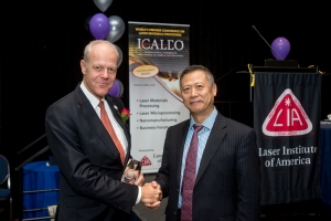
Laser Institute of America presented Professor Reinhart Poprawe, managing director of Fraunhofer Institute for Laser Technology (ILT), the Peter M. Baker Leadership Award during this year’s International Congress on Applications of Lasers & Electro-Optics (ICALEO®) in Atlanta, Georgia, Oct. 22-26.
Lin Li (right), former LIA president, presented LIA’s Peter M. Baker Leadership Award to Professor Reinhart Poprawe(left), at ICALEO, Oct. 25 in Atlanta, Georgia.
The award acknowledges individuals who demonstrate outstanding leadership in an organization while significantly benefiting the laser community. It is named after former LIA executive director, Peter M. Baker, who led LIA for almost three decades.
“There is no question that Professor Poprawe richly deserves this award. In our world of lasers, he is a leader on the grand scale, technical, organizational, political and social,” Baker said. “He is a fine gentleman, courteous, thoughtful, generous and funny. I consider it an honor to be his friend.”
Poprawe’s professional expertise includes laser applications, laser additive manufacturing, and photonics in life science. Additionally, he has a great deal of experience in laser development and plasma technology in the realms of process analysis, sensors for laser processes, laser induced plasmas and more.
“The award is from one of the most important laser communities in the world,” Poprawe said. “It is a great honor to receive this award as the first recipient after the original, Mr. Peter Baker himself.”
According to several of his peers, Poprawe has been an important figure within the industry for decades.
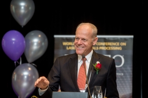
Professor Reinhart Poprawe addresses a crowd at ICALEO, Oct. 25 in Atlanta, Georgia.
“Professor Poprawe has been an important figure here at LIA for years,” said Nat Quick, LIA’s executive director. “He has been an LIA board member since 2001 and he always steps up when it counts most. He served as an LIA president in 2012 and has functioned as editor-in-chief of the Journal of Laser Applications® (JLA) since 2010. He is incredibly generous and exemplifies what it means to be a leader.”
After earning his Physics Ph.D. in Germany, Poprawe worked as the laser-oriented process development department head for Fraunhofer ILT before becoming their managing director. Additionally, he holds the university chair for Laser Technology at the RWTH Aachen University.
“There are so many ingredients for a successful organization,” Poprawe said. “Vision; mission; research and product portfolios; roadmaps; SWOT-analysis; and education of the employees. Industry or even better societal use and implementation of our research results is what we do everything for, especially the development of the demanding competencies in the very fundamentals of Laser Technology and application Physics.”
About LIA
The Laser Institute of America (LIA) is the professional society for laser applications and safety serving the industrial, educational, medical, research and government communities throughout the world since 1968. www.lia.org, 13501 Ingenuity Drive, Suite 128, Orlando, FL 32826, +1.407.380.1553.
Fig. 1: Setup configuration for 3D polishing and structuring
Surface preparation can have different properties for a large field of applications in very different industries.
Polishing a surface can avoid unsightly defects on mold parts, or can provide very smooth surfaces for finished products. Since actual ablation processes are time-consuming, can create dust and at times involve chemical treatment, a new approach of using direct laser surface modification has a great market potential.
Industrial fiber lasers can be competitive by melting and smoothing the surface up to 20 times faster than conventional techniques, and their costs are lower than pulsed lasers.
But sometimes surfaces need to be machined to replicate patterns on a part. This method is often used in various industries such as automotive (for dashboards) and injection molding. Laser ablation is already used to design complex patterns but their ablation rates are low: Nanoseconds lasers obtain volume rate ablation close to 1mm3/s but laser remelting can reallocate metal and create a pattern 30 times faster without the need of finishing process due to the surface tension the resulting surface has a polished like finish.
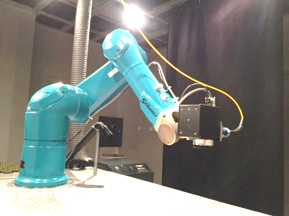
The setup is quite industrial with a fiber laser from IPG (YLR 300/3000 QCW -1070 nm multimode, 300CW, 0.1-10 ms) plugged into a PRECITEC F100 collimator and mounted onto a SCANLAB Hurryscan III 14mm galvanometer scanning head providing a scanning speed up to 2.5 m/s.
To obtain a full 3D solution, the scanner has been mounted on a STÄUBLI Robot (TX90-L) which can treat parts within volumes up to 1 m3.
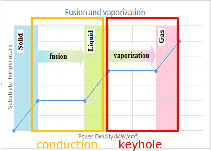
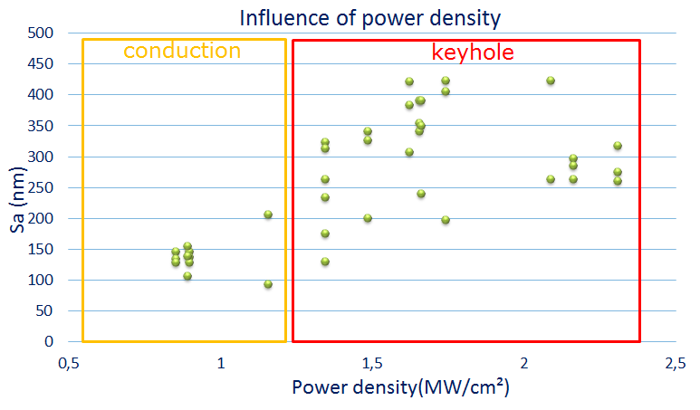
The optical configuration and the control of the laser power allow the user to determine the metal modification. With low or modest laser power density that irradiates the sample, the metal reaches melting temperature, whereas at high power density vaporization temperature is reached. These two different temperature profiles will lead to conduction mode melt formation or keyhole formation, respectively (Figure 2).
Fig. 2: Both welding modes: Conduction and Keyhole
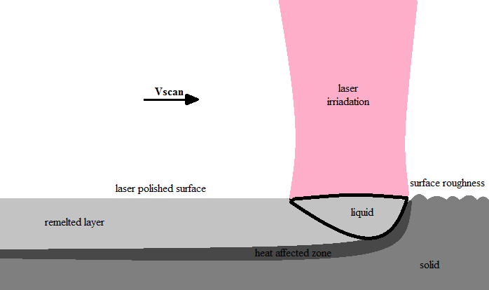
Fig. 3: Mechanisms of laser polishing
Polishing metal is achieved by irradiating the sample with a laser beam in order to melt a thin metal layer. Therefore, the melted metal peaks fill the valleys, and when solidifying, the surface tension smooths the metal hence reducing the roughness (Figure 3).
If the laser power is not constant during the processing, the melt pool volume varies as the power increases or decreases (Figure 4). Furthermore, due to changes from solid to a liquid phase and the thermal dilatation, the melt pool surface bulges outward. By this way, patterns can be created by modulating the laser power.
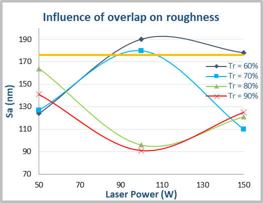
Fig. 5: The influence of overlap in reducing the roughness
Fig. 4: Mechanisms of laser structuring
Plenty of parameters were tested on stainless steel (304L) in order to identify the main trends, to obtain the melting pool and to reduce roughness. The first goal was to find the best line overlap. Experiments were made for laser power from 50 W to 150 W, while overlap varies from 60% to 90%. The best operating range was identified for overlaps between 80% and 90% (Figure 5).
Secondly, by tuning laser power and beam diameter, the laser power density varies. We underline that best results are obtained with power density from 0.8 to 1.2×10⁶ W/cm² which corresponds to conduction mode welding. While increasing the laser power density, keyhole welding quickly appears resulting in higher roughness (Figure 6).
Fig. 6: Welding mode depending on the laser power
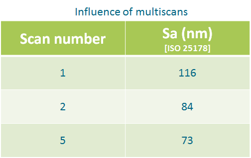
Fig. 7: Roughness reduction with multiscans
The third main parameter affecting roughness was identified to be the number of scans (Figure 7). Multiscans can slightly reduce the final roughness, and best results are obtained by crossing the hatch by 90°.
Applying these main parameters on surfaces with varying degrees of roughness produces smoother surfaces. Bright surface aspects are obtained with processing times from 20 s/cm² to 200 s/cm² depending on the initial roughness.
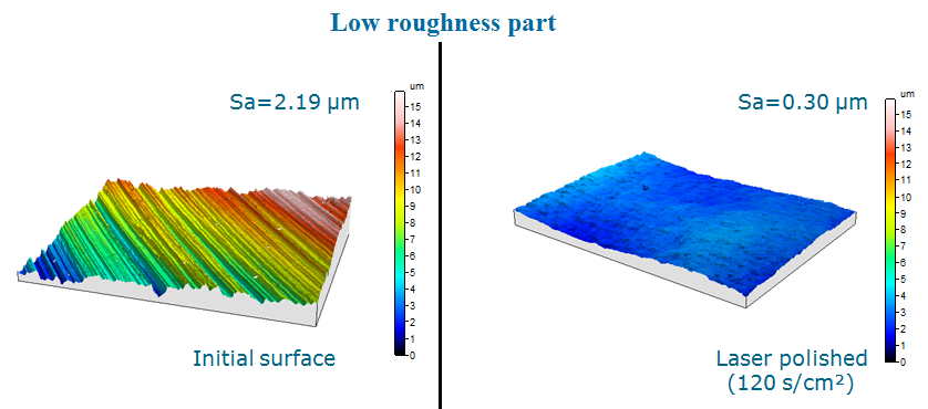
Fig. 9: Low roughness part polishing
Fig. 8: High roughness part polishing
On high roughness parts with a Sa value of 6.4 µm (Figure 8), the roughness can be reduced by 10 within a processing time of 200 s/cm². This could be a good way to pre-reduce the roughness in a very short processing time. In this case, the heat affected zone is around 320 µm.
Fig. 10: Polished area on stainless steel
On most common milling parts roughness is around 2 µm (Figure 9). In this case, processing time is close to 100 s/cm², and the heat affected zone is reduced (around 35 µm). Laser polishing can then reduce the roughness by 8 times, producing bright surfaces (Figure 10) and can find applications in fine polishing to obtain reflective surfaces.
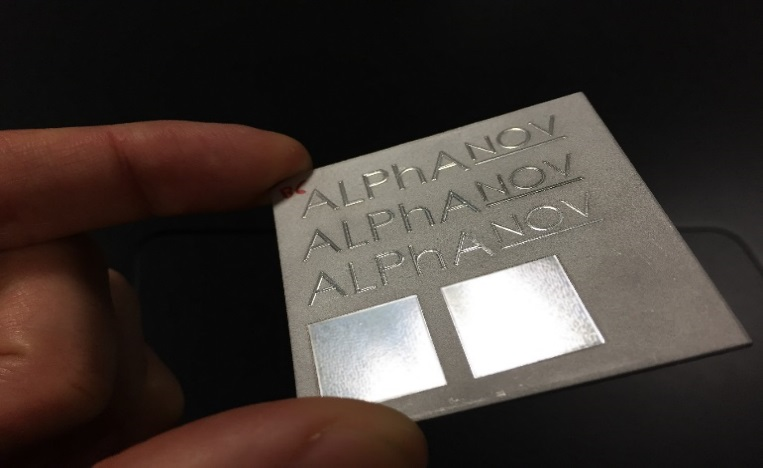
As the laser treatment possesses a high resolution, selective polishing can be made to create high contrast for patterning and writing texts to preserve sharp edges on a part and reach areas with difficult access where conventional tools cannot be employed. This versatile solution can produce details around 1 mm² and find decorative applications.
Fig. 12: Selective polishing on sandblasted aluminum
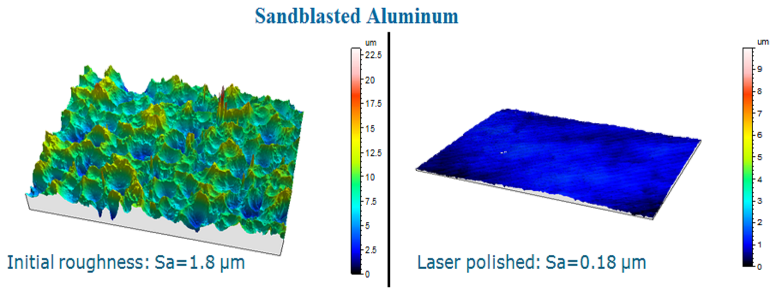
Fig. 11: Sandblasted Aluminum polishing
This case was tested on a sandblasted Aluminum surface whose roughness has been reduced by 10 (Figure 11) resulting in a very reflective surface (Figure 12).
Laser polishing offers various possibilities in pre-polishing or fine polishing in many applications from molds (injection, glass, etc.) to decoration.
According to the previous observations on polishing metals, laser power density can vary between the melting point and vaporization point to control the melting pool volume and imprint into the metal surface a 3D pattern by reallocation of the melt volume and resolidification in different locations.
Fig. 13: Quick modulation profile
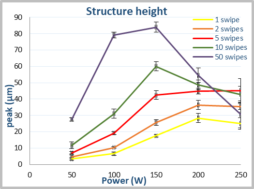
Fig. 14: Swipe number influence on peak height
In the first modulation profile, we apply full laser power along the first millimeter, then the laser is switched off along the following four millimeters (Figure 13). The peak height is measured from laser powers ranging from 50 W to 250 W and swipe numbers from 1 to 50 (Figure 14).
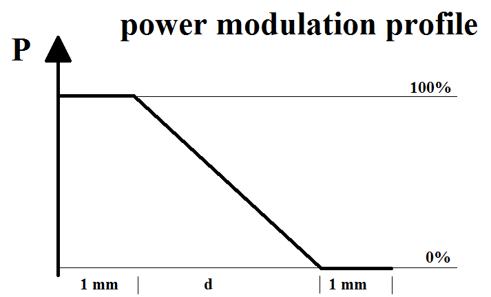
The peak height increases with the laser power and the swipe number, but above a power of 150 W and for swipe numbers over 10 swipes, the peak height decreases due to heat accumulation. In order to enhance the buildup, experiments are made with a new power modulation profile. Now, laser power decreases along a distance, ‘d’, from 1 to 10 mm (Figure 15).
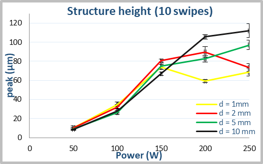
Fig. 16: ‘d’ distance influence on peak height
Fig.15: Slow power decrease modulation profile
By using this new power profile and 10 swipes, the peak is still growing over 150 W for distances over 5 mm. For shorter distances, heat accumulation is observed, which reduces the peak height (Figure 16).
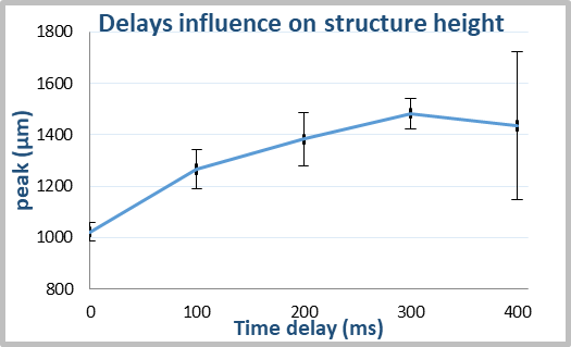
Fig. 17: Delay influence on peak height
Fig. 18: Peak’s shape without and with delay
To avoid heat accumulation influence, a delay between each swipe is introduced for 200 swipes and laser power of 250 W (Figure 17). Without any delay, the peak height reaches 1 mm. However, introducing a 100 ms delay results in the height growing by 25%, and by 50% with a 300 ms delay. The peak’s shape without delay is rounded, with oxidation and spatters around, meaning that the welding process turned into keyhole mode welding due to heat accumulation (Figure 18 left). With a delay or oxidation, the peak is higher and the shape is like the power modulation profile (Figure 18 right).
Modulating the laser power combined with a scanning strategy permits the creation of complex patterns (Figure 19) up to 30 times faster than by laser ablation processes.
Fiber lasers are perfectly adapted for polishing with good results in a very short processing time. Depending on the initial roughness, the processing time varies but can be approximately 20 times shorter than conventional processes, and the remelting produces no dust or other side effects that require posttreatment.
By modulating the laser power, it provides a low-cost alternative in comparison to short/ultrashort pulsed laser for engraving and patterning applications with processing speeds that are 30 times faster, while keeping the polished appearance directly after the pattern generation. Depending on the strategy, we can create a micro structure (some µm) and macrostructure (over millimeter) topographies.
Christophe ARNAUD christophe.arnaud@alphanov.com is a technician in the laser micromachining business unit at ALPhANOV working on meso-scale laser processes.
By: Thomas Schopphoven, Fraunhofer Institute for Laser Technology ILT
Coatings for Wear and Corrosion Protection
When the integrity of a component is affected by the operational conditions, it may become necessary to additionally protect the material against this detrimental environment. Since most material damage processes, especially wear and corrosion, emanate from the surface or near surface regions, the application of coatings is the most suitable route to protect metallic surfaces. Coatings designed for the wear and corrosion protection must be an effective physical and chemical barrier, preventing the aggressive influence to the base material. The required thickness of the coating is dependent on the particular application and can range from a few up to several hundreds of micrometers. Generally, each coating system is aimed for specific functionalities, which among others include the chemical composition of the coating material, the adhesion to the base metal, the microstructure, the corrosion inhibition and the wear resistance.
While wear and corrosion protection coatings contribute to the performance, reliability and service life of many components across all industrial branches, these benefits often must be weighed against the environmental damage. For many years the most effective wear and corrosion protection systems were based on the use of chromate-rich surface treatments which turned out to potentially cause health problems for production workers and the community as a whole. The current legislation imposed by REACH (Registration, Evaluation, Authorization and Restriction of Chemicals) now prohibits the use of hexavalent chromium in almost all sectors. Similarly, this restriction applies to the use of nickel in electroplating, which has been classified as dangerous for the environment and toxic by the WHO (World Health Organization). As a result, REACH decisions have fostered the search for more advanced “green,” non-toxic and resource conscious coating technologies for the wear and corrosion protection. Many alternatives have been investigated, and so far the most promising technologies are thermal spray technologies, especially high velocity oxygen-fuel (HVOF) thermal spraying and laser material deposition (LMD).
The Search for “Green” Alternatives
Fig. 1: Cylinder in the paper making industry (Diameter: 1.000 mm, Length: 10 m)
With HVOF thermal spraying, coatings out of a large range of materials can be applied, featuring a high wear resistance at relatively high deposition rates (1-4 kg/h). However, thermal spray coatings are technologically constrained in regards to the limited adhesion strength due to the poor mechanical bonding between coating and substrate. Moreover, thermal spray coatings are difficult to repair and often exhibit porosity levels in the range of 1-2%, lowering their corrosion resistance. Another disadvantage associated with HVOF thermal spraying is the comparatively high resource consumption of fuel, powder and oxygen. With LMD high-quality, almost 100% dense, pore- and crack-free coatings out of a wide variety of materials can be produced with a strong metallurgical bonding. Through a defined heat input and localized material deposition, LMD provides remarkable benefits over conventional welding processes and thermal spray technologies. Due to the very small heat input, a rapid solidification and a fine microstructure can be achieved with a property profile that meets, or even exceeds, the specifications of wrought or cast material. However, for the coating of large components, such as cylinders in the paper making industry (Figure 1), the LMD process is too slow (coating rate: 10-50cm2/min, deposition rate: < 0.5 kg/h). Furthermore, LMD layers are too large for many applications (>500 µm). In this layer thickness range, many conventional welding technologies, such as tungsten inert gas welding or plasma powder welding, offer cost advantages due to drastically lower investment costs. Various facilities and companies already addressed the reduction of processing times in LMD over the past years, by producing larger melt pools with higher laser powers in order to deposit more powder per time. In fact, the deposition rate could successfully be increased, but in turn the resource-consumption, as well as the heat input, was increased. The core issue—the simultaneous reduction of the layer thickness and coating time—could not be solved.
Ultra-high-speed LMD: The first economical coating process for thin, metallurgically bonded layers
Fig. 2: Top: Schematic process principle for conventional LMD; Bottom: Schematic process principle for ultra-high-speed LMD
The maximum process speed as well as the minimum layer thickness in LMD is limited, because the heating and melting of the powder particles in the melt pool require a certain time and melt pool size. In Fig. 2 on the top, the process principle of LMD is schematically shown. Because the powder focus of conventional powder feeding nozzles is comparatively large (2-3 mm), most of the laser energy is transmitted to the substrate. As a result, most of the particles entering the melt pool have a considerably lower temperature Tp than the temperature of the liquid melt pool Tliq (Tp < Tliq). The general approach in ultra-high-speed LMD is to already heat the powder particles to melting temperature before they enter the melt pool (Tp ≈ Tliq), see Figure 2. To this, a larger amount of optical energy is deposited into the powder gas stream. At the same time, only a small fraction of transmitted energy is used to produce a thin melt pool on the surface of the substrate. Since both the necessary time and melt pool size are drastically reduced, a simultaneous increase of deposition speed by orders of magnitudes and the reduction of layer thicknesses to 10-250 µm can be achieved. Since less energy is deposited into the base material, only a very small heat affected zone (HAZ) and bonding zone with low dilution is formed. In order to deposit more energy into the powder gas stream, special powder nozzles are required, which produce a high optical density and a small powder focus diameter (0.5-1 mm).
Ultra-high-speed LMD for Internal Surfaces
Fig. 3: Schematic of inside processing head for ultra-high-speed LMD with integrated continuous coaxial powder nozzle
For ultra-high-speed LMD on outside diameters, standard optics and can be used for the processing of internal surfaces, i.e., for the coating of cylinder sleeves, bearings and housings of the oil and gas industry or plastic and extrusion components. However, special processing heads are required. The optical components, the powder feed, the water cooling system and the tubes for the shielding gas have to be integrated into a compact housing. For conventional LMD various processing heads for different inside diameters and immersion depths have been developed and are used in industry. Due to the limited available space, up to now only multiple-jet coaxial or lateral powder feeding nozzles are used for internal LMD processing heads. However, the required small powder focus diameters for ultra-high-speed LMD can currently only be achieved with coaxial powder feeding nozzles with a continuous powder gas stream. Based on the basic principles continuous coaxial powder feeding concepts for the ultra-high-speed LMD on outside diameters, Fraunhofer ILT developed a novel continuous coaxial powder feeding nozzle and adapted it for an inside LMD processing head from IXUN Lasertechnik, see Figure 3.
Fig. 4: Left: Inside processing head integrated into the ultra-high-speed LMD system; Right: Process image of ultra-high-speed LMD on an internal surface; Bottom: Cross-section of an ultra-high-speed LMD layer
The inside processing head is integrated into a Hornet Laser Cladding high-speed LMD machine, see Figure 4, left. The system is based on a conventional lathe and retrofitted for ultra-high-speed LMD of rotationally symmetric components. With the system technology sound wear and corrosion protection layers in the thickness range of approximately 50-350 µm can successfully be deposited on the internal surface of cylindrical tubes with a minimal inside diameter of 100 mm with coating rates up to 200 cm2/min and deposition rates up to 1.5 kg/h, see Figure 4 on the right. On Figure 4 on the bottom a cross-section of a sound, metallurgically bonded ultra-high-speed LMD layer with minimal dilution and a thickness of approximately 100-150 µm is depicted.
Dipl.-Ing. Thomas Schopphoven is a Research Associate at Fraunhofer ILT and an expert for Ultra-high-speed Laser Material Deposition.
Orlando, FL (October 23, 2017) – After almost three decades, the Laser Institute of America is making an enormous change by appointing Dr. Nathaniel Quick, founder of AppliCote Associates, LLC and former LIA President, as its new executive director. Quick will succeed Peter Baker, who retired in May of this year.
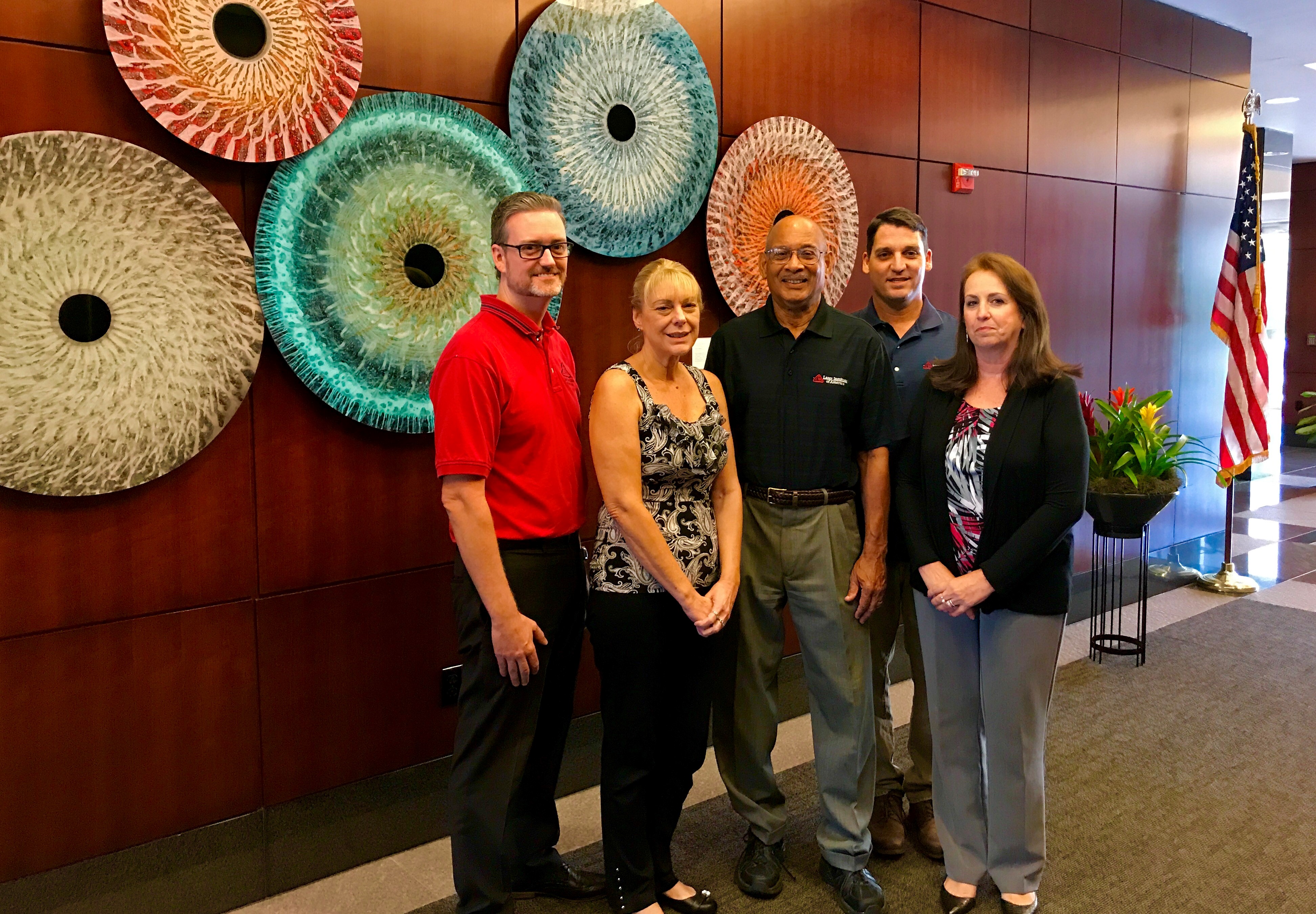
Dr. Nat Quick poses for a picture with LIA leadership, in Orlando, Florida Oct. 19. Quick is the association’s new executive director.
“We are grateful for the 28 strong years Peter Baker gave us at LIA,” said Paul Denney, LIA President. “And we are excited to grow LIA with Dr. Quick’s extensive leadership and experience. LIA will continue to lead the industry just as it has for many years.”
Quick takes the helm this year after his nomination by LIA’s board of directors; he is expected to lead the association for the next several years.
“I welcome this opportunity to guide LIA in this phase of its innovative growth,” Quick said. “LIA has been a tremendous laser materials processing knowledge-base for my company, inspiring the creation of our patented laser based technologies for new industrial applications. Now, I can repay the favor.”
Quick earned several degrees in Materials Science and Engineering from Cornell University including a Doctor of Philosophy, which he received in 1976.
After completing his education, Quick held a position as the Vice President of Washburn Wire Products, Inc., where he focused on quality control and laboratory operations. Eventually, Quick cofounded AT&T Coatings, an entrepreneurial spin-off with a focus on technological applications.
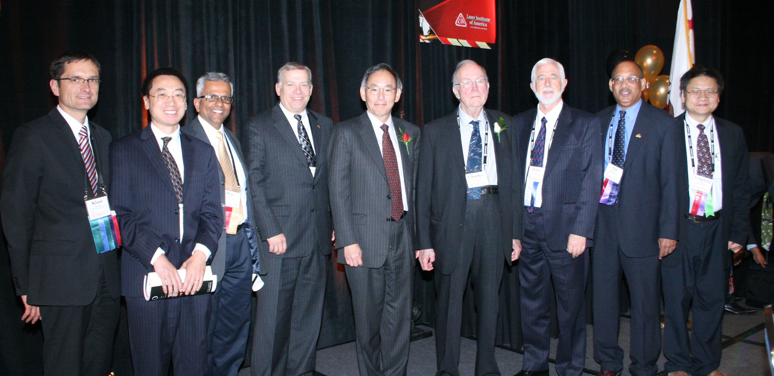
Dr. Nat Quick, second from the right, with Charles H. Townes, Peter Baker and LIA’s board of directors at ICALEO 2010.
Between 1985 and 1989, Quick was the CEO, and chief scientist for his own company, Applications Technology of Indiana, Inc., where he invented and/or developed clad-coat micro-composited powders for powdered metal and conductive polymer electronic applications. From 1990 to 2002, Quick filled leadership positions within several companies that concentrated on materials processing and research development. For several years he continued to hone his skills as a negotiator and a project developer before founding his self-financed company, AppliCote Associates, LLC, in 2003.
Quick hopes to bring his appreciation for science and technology to LIA and its employees.
“LIA has the opportunity to become the portal to all industries and personnel that want to access laser information,” Quick said. “We are developing the means to better deliver data related to laser technology and innovative applications internationally. In short, we are becoming the content provider for all laser based technologies.”
Dr. Nat Quick and his wife at a local martial arts school Quick attends often. He said he enjoys martial arts because of its physical and mental benefits.
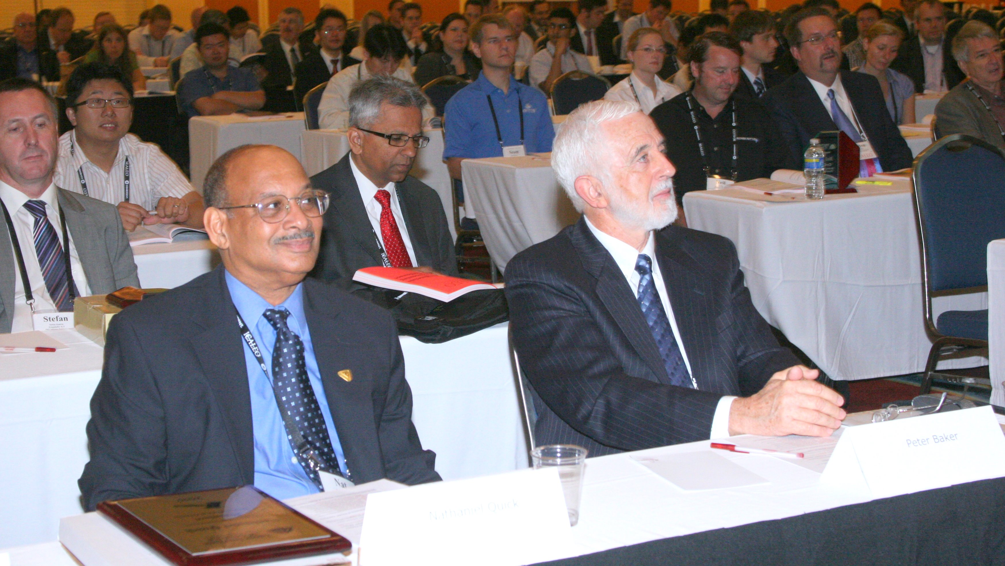
Dr. Nat Quick (left) and former LIA executive director, Peter Baker (right) observe a presentation at ICALEO 2010. Quick was the president of LIA at the time.
About LIA
The Laser Institute of America (LIA) is the professional society for laser applications and safety serving the industrial, educational, medical, research and government communities throughout the world since 1968. www.lia.org, 13501 Ingenuity Drive, Suite 128, Orlando, FL 32826, +1.407.380.1553.