Laser Micromachining of Transparent Dielectrics – Glass and Quartz Using Nano Short Pulsed Nd: YVO4 Laser Harmonics

By Shiva Gadag, Radovan  Kovacevic and Nilesh  Ramani

Introduction:
Glass, Quartz, and Silicon are made out of sand grains consisting of Silica, SiO2. Silicon and Glass are two basic building blocks which go hand-in-hand in the fabrication of optoelectronics and microelectronics device for MEMS and Biomedical microdevice applications such as charge coupled device, lab-on-a-chip, microsensors, microfluidic arrays, PV solar cells etc.

Miniaturization of microelectronics device is the driving force for laser micromachining of transparent dielectric Glass, Quartz and semiconductor Silicon materials. The dawn of digital era has diminished the dimensions of digital devices to micron and submicron scale resulting in shrinking the size of silicon and its dioxide dielectrics based digital devices much faster than the predicted ones by the Moore’s Law. In order to meet the digital demands of the 21st century digital revolution, laser micromachining or laser lithography is the only workhorse for alternative noncontact toolless techniques for digital device micro-manufacturing. Laser micromachining with shorter pulse widths result in accurate spatial resolution, precise depth control, enhanced edge quality and minimal peripheral damage. On the other hand conventional mechanical machining of transparent dielectrics and semiconductors is economically expensive and time consuming due to the hardness and brittleness of these materials. Nano short pulses and Ultrashort pulses are most commonly used for micromachining of transparent materials. The microprocessing of hard and brittle transparent materials is accomplished due thermal ablation by heating and evaporation of surface atoms in the former laser process. The nanosecond laser micromachining can often induce some undesirable heat affected zone surrounding the feature. Whereas in the latter process, the photoablation directly results in material vaporization by breaking the atomic bond by stripping electrons. The ultrashort micromachining is cold ablation with negligible heat affected zone due to no heat transfer to surrounding area. However, ultrashort micromachining techniques are quite expensive for industrial processing of glass such as cutting, drilling and marking for touch screen glass panel displays, microfluidic chambers, solar panels and microlens and optical components for photonics industries. As a result ultrashort processing is ideal only for applications demanding extreme precisions and excellent quality with negligible HAZ. However, a similar precision and quality of micromachining of transparent, hard and brittle materials can be achieved with nanosecond short pulsed lasers but with some traces of HAZ. The nano short pulsed lasers are relatively less expensive as compared to ultrashort lasers but far more efficient than the conventional machining methods. Hence the purpose of this article is to demonstrate the ease and efficacy, pros and cons of nanoshort pulsed lasers in micromachining of transparent and brittle materials like glass and quartz using Nd: YVO4 laser harmonics.

Experimental Technique:
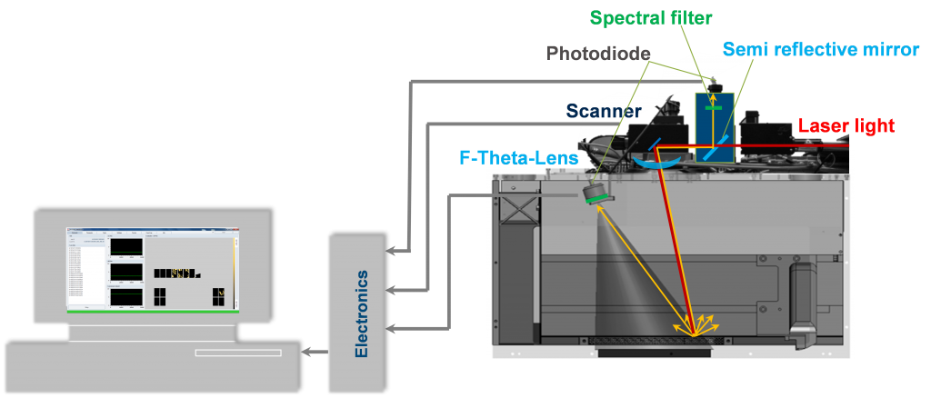
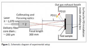
The micromachining system (Figure-1) used nanosecond pulses (11ns duration) of Nd:YVO4, DPSS, Q-switched, HIPPO laser with four harmonics generating fundamental IR λ=1064nm, 2) Green λ=532nm, 3) UV λ=355nm and 4) UV λ=266nm respectively. The micromachining gantry consisted of X,Y,Z stage with laser mounted on the top tier was focused after 8X beam expansion by

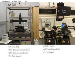
Figure 1 – Laser micromachining work stage (left) and experimental setup (right) to measure laser power transmittance in glass.

telescopic lens and 90o reflections by 2 mirrors on incoming beam opening of HurryScan-II. The scanner focused beam to diffraction limited spot diameter, d=18 microns using 100mm telecentric lens and rastered beam as per CAD feature on substrate view field of 45mm. The substrates were 1mm Corning#0215 glass and 2mm photolithographic Quartz. PerkinElmer LAMBDA UV/Vis/NIR spectrophotometer was used to determine transmittance of glass for the range of wavelengths covering four laser harmonics. Glass being transparent (T>90%) IR and green wavelengths, the first two harmonics are not suitable for micromachining. The absorbance of UV wavelengths being A>75% , the third and fourth harmonics are better suited and fourth harmonic UV λ=266nm is most ideal among the four harmonics for micromachining of glass.

Defect Diagnosis of Dielectrics:

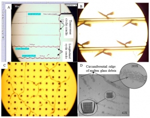
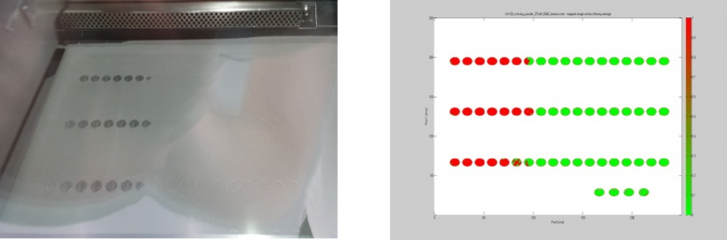
Figure 2 – The defect diagnosis of laser induced cracks showing A) regular cyclic cracks formed by primary mode-I type of precrack, B) regular periodic nodes of Butterfly type of cracks, C) Colony of Crack grain boundary surrounding the vias and D) concentric circles of dentritic debris of droplets of molten glass

Hence UV laser was used for micromachining of glass and quartz but the initial trials with high diode current resulted in various types of defects shown in the Figure 2. Systematic analysis of the defects formed in glass during micromarking and drilling revealed two types of crack formation, namely periodic and irregular type of cracks. The primary mode-I crack formed during marking of parallel lines with high diode current at high repetition rates, propagated as cyclic crack with a well-defined wavelength of propagation all along the length of the parallel lines on glass while micromarking, The cyclic micro cracks formed by primary mode-I crack either propagate as secondary sinusoidal crack with a wavelength of propagation proportional to the wavelength of laser harmonics. Alternatively primary precracks propogate as tertiary transverse cyclic cracks along the transverse line of laser marking with a wavelength equal to perpendicular distance between the parallel lines of laser marking. The second type of periodic cracks appeared as periodic nodes of cracks at regular interval resembling tiny butterfly. The irregular type of cracks formed crack grain boundary during laser drilling of microvias on glass due very high diode currents or pulsing frequency. The irregular cracks formed colonies of cracks surrounding the microvia. The expulsion of molten glass debris often solidified as concentric circles of dendritic glass droplets surrounding the circumference of the micro vias array formed on glass.

Optimum Power, Frequency and Wavelength of Laser:
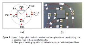
Apart from the transmittance of various wavelengths in the glass, absorbance of a suitable wavelength and its response to average power and pulsing frequency of the laser is crucial for micromachining of the glass without any defects or cracks. To establish the power and frequency response to absorbance of the laser, average power transmittance characteristics of glass for the laser harmonics were determined using the setup shown in the Figure 1. The diode current of the diode pumped solid state laser is directly proportional to average power of laser harmonics. As the diode current increased from 1 to 100% , the average power laser harmonics linearly increased to 17.5W for IR and 8.5W for Green, 5W for UV λ=355nm and 2.5W for UV λ=266nm respectively. Since absorbance characteristics of laser to diode current and frequency of pulses being identical for all four harmonics, second harmonic green laser λ=532nm was chosen to study the power and frequency response to absorption of the laser.

Intensity, I0 of power incident, P0 on glass in air, I0 = P0/(pr2) and transmitted intensity, IT of power, PT through glass IT= PT/(pr2) were measured by thermopile sensor. Applying Beer-Lambert’s law due to high optical penetration of the glass, absorption coefficient of the laser in glass thickness, l was calculated using b =-ln(IT/I0)/l . Diode current and frequency response of laser absorption in Corning glass measurement (Figure 3) indicated optimal laser power for 60-70% diode current and frequency of 55 kHz for effective micromachining.

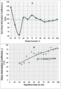
Figure 3 – Measurement of absorption coefficient of Corning glass as function of A) Diode Current and B) Pulsing Frequency (kHz) of HIPPO Laser.

Results:
Finally using the suitable wavelength (λ=266nm) and optimal energy (5-10 µJ) and frequency (50 kHz) of 11ns short pulsed UV laser, cracks were eliminated and defects were minimized in micromachining of glass. The process optimization enabled to get fine parallel lines of 17µm and arrays of microvia of 15µm diameter at 75µm pitch, as well as etching and scribing without any cracks on glass (Figure 4). This helped to make microchannels and microfluidic tubes in 2mm thick quartz using nanosecond pulsed UV laser.

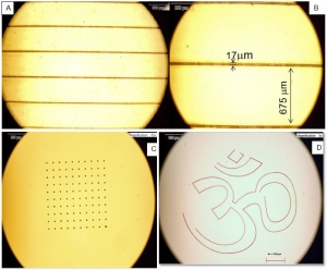
Figure 4 – Optimization of laser parameters enabled crack-free micromachining of glass: A, B) Fine line marking, C) drilling of microvias, and D) etching and scribing of glass.

Conclusion:
An optimization of laser process parameters – wavelength, power and frequency nanosecond pulse laser crucial critical factor for micromachining of transparent dielectrics of glass and quartz with minimal HAZ, less defects and relatively free from flaws and cracks. The technical feasibility of the cost effective nanosecond pulsed lasers in microprocessing of transparent dielectrics is clearly established in this article.

Professor Radovan Kovacevic is with Dept. of Mechanical Engineering, Southern Methodist University, Dallas TX and Shiva Gadag is with ScanTech Lasers Pvt. Ltd. Nilesh Ramani is Director & CEO of Scantech Laser Pvt Ltd, India.

Diode Lasers in Cladding, Additive and Hybrid Manufacturing

By Oleg Raykis

Today there exist a number of technologies for additive manufacturing of components.

The two most prominent types utilizing lasers for generating parts out of metals are either powder bed based solutions or direct energy deposition, often referred to as laser metal deposition. As a company Laserline focuses mainly on the second type. Depending on the application it allows you to produce larger part sizes with higher productivity (deposition rates and therefore higher productivity) due to the fact of not being limited by the size of the building chamber as it would be in the case of a powder bed machine. It is also much faster in many cases.

Laserline identified four main application areas for AM in which we operate and be described based on examples in this article. Those areas include, besides generating complete parts by terms of additive manufacturing, also repair welding application or hybrid machines – a combination of conventional machining and laser technology the fourth main application area would be providing functional areas on conventionally manufactured parts.

Additive manufacturing technology allows generating shapes and structures in a single production step with little material loss, post machining and tool wear (near-net-shape manufacturing). Thereby you can use material in powder or wire form. The advantage of using wire is that you will have a 100% material utilization; the compromise on the other hand might be the directional dependency when you supply the wire laterally and not coaxial. Pic. 1 shows an example of a free form application as a rocket nozzle demonstrator part made out of Inconel 625.

Pic.1 Free form powder AM of a rocket nozzle demonstrator (Source: Fraunhofer CLA)

The part was done without any type of process control. Another interesting example of AM with Titanium is shown in Pic.2.

Pic. 2 Ti64 powder AM with closed loop process control (Source: Fraunhofer CLA)

Compared to the rocket nozzle, process control was used when producing the demonstrator part in pic.2. The camera based system (in this case E-MAqS) is capable of measuring the size and temperature of the melt pool. Furthermore it can give feedback to the laser source and adjust the laser power accordingly to maintain the desired size of the melt pool. This in turn ensures consistent reproducible part build ups with no defects.

Another very interesting and promising approach is to integrate the laser source into machine tools. There are several hybrid machine tool concepts being developed; one of them is the combination of additive and subtractive tools which achieves a new level of manufacturing. One example is the merger of a laser with a 5-axis milling machine. The integrated diode laser deposits the powdered metal layer by layer, generating a solid, fully dense metal part. The following milling operations directly finish machines surfaces in areas necessary, without changing setup.

Pic.3 An example of a conventional milling machine with integrated AM technology (Source: DMG Mori-Seiki)

This flexible switch between laser and mill also allows the machining finish of areas, which would be impossible to reach on the final component. Designs with undercuts, internal geometries and overhangs without support structure are no problem. The manufacturing of completely new structures and designs are now possible. All weldable metals, which are available in powder form, can be used, for example steel, nickel and cobalt alloys as well as titanium, bronze or brass.

A third important field of AM from our perspective are repair welding applications. Probably the most prominent and widely industrially utilized are the repairs of turbine blades. Turbine blades in steam engines, especially in the first two rows, experience a lot of wear through erosion. Instead of replacing the whole part it is possible to repair the worn area by putting a couple of layers (mostly nickel / cobalt based super alloys) and machine them down to the finished surface, see Pic.4.

Pic.4 Turbine blade repair (Source: Fraunhofer ILT)

This remanufacturing procedure saves up to 90% of material and energy cost compared to manufacturing a new blade. Even though turbine blades are the most prominent example of laser repair welding a wide variety of other parts can be restored using the procedure, e.g. worm shafts, helical gears, molds, etc. to name a few. When speaking about additive manufacturing most people have the production of complete parts in mind. This doesn’t always have to be the case. Often it makes more sense from an economic standpoint to add to a conventionally (and relatively inexpensively) produced part functional areas where they are needed. Pic. 5 shows one such example.

Pic. 5 Extruder barrel demonstrator (Source: Fraunhofer CLA)

In this case 100 lbs. of hard and wear resistant Stellite 21 powder material was deposited on a metal pipe base structure to form the extruder thread. One further example of it can be functional layers on drill bits where sensors need to be shielded from magnetic interference. By creating heat resistant layers out of non-magnetic materials it is possible to place those sensors.Through a clever combination of the usage of conventional and additive manufacturing technologies it is possible to produce advanced parts without increasing the cost.

Quality Assurance of Selective Laser Melting Applications

By Thomas Gruenberger

Key differentiation criteria for Additive Manufacturing (AM) technologies are freedom of design, cost advantage, customization, and time to market.

Direct metal laser sintering (DMLS) AM technology is ideal for serial production for industries like aerospace.

Setting up a process means mapping the input parameters (e.g. machine and process parameters and part geometry) to output parameters (part properties like density, tightness, surface quality). An in-situ nondestructive measurement of part properties like density is not possible, so indirect measurements have to be performed. Information from the process – process emissions, melt pool size, melt pool dynamics, and temperature distribution – can be used for this indirect measurement enabling the user to find a correlation between features of these measurements and the resulting part properties. Additionally, a shorter process development time can be achieved by avoiding destructive tests during development learning reading the extracted features (see Fig. 1).

Fig. 1: Quality inspection – the challenge

As mentioned above, several pieces of information from the process can be used for the detection of irregularities, so different sensor technologies can be used. Consider a manual in-situ inspection of the process, where the user looks at the visible process emissions in the process chamber. Differences in brightness, size, color, and number of sparkles can be detected with the human eye. This can be automated using photodiode based meltpool monitoring systems like the plasmo fast process observer, a hardware developed by plasmo with up to 4 channels at sampling rates up to 300kHz.

So the system measures the brightness of the process emissions over time (blue curve in Fig. 2), using CAD data, the data can be mapped easily to an image of brightness of process emissions over the building platform (see Fig. 2 right plot), layer for layer, in pseudo color representation.

Fig. 2: Feature map of the building process

Running an OK process gives the baseline of the feature, provoking process irregularities yields in a change of the feature, enabling the user to set limits for the feature according to its quality needs. A pseudo color representation of a map of process irregularities can be calculated, giving the user an easy way to understand visualization and therefore, fast feedback about the quality of the process. As a note, black means no process irregularities and yellow means 100 percent of process irregularities in the given pixel in Fig. 3.

Fig. 3: Map of process irregularities

The fully automated measurement system enables a 100 percent inspection of the building process. The high sampling rate (ca. 10,000 times fa

ster compared to the human eye) enables the system not only to calculate features like signal height but the additional analysis in time, frequency and time scale domain can be performed, too. Three (3) different algorithms (features) are calculated by the system and each algorithm can be parametrized according to the quality needs for every exposure type used in the layer.

These algorithms are easy to explain. Based on physics, they correspond directly to process different phenomena.

  • Absolute limits: Influences in the size and form of the cross section of one exposure like focal position, laser power and welding speed
  • Signal dynamics: Noisy processes or less process dynamics like pollution, protective gas flow and lack of fusion
  • Short time fluctuations: Short changes in the signal caused by e.g. ejects and pollution

In cooperation with EOS, the described system was integrated with their machines. A typical layout is shown in Fig. 4.

Fig. 4: System layout – EOSTATE Meltpool

As shown in Fig. 4, two total photodiodes are used an onAxis diode measuring the process emissions at the interaction zone of the laser beam and powder and an offAxis diode giving an overview of process emissions about the complete building platform.

A heuristic model is used for setting up the system; therefore, input parameters like process parameters (laser power, scanning speed, gas flow, …) and malfunctions like loss of laser power, and material quality are varied for different building jobs. The output parameters are part properties (porosity, surface roughness, …), process emissions (brightness, temporal behavior, spectral properties, …) and undesired effects like overheating, warpage and lack of fusion. Based on this data set the system can be parametrized to fulfill the quality needs of the customer.

Fig. 5 shows a provoked malfunction, missing powder choosing a too low dosing factor of powder, the irregularities (here red in Fig. 5) can be easily detected.

Fig. 5: Example missing powder, left image of powder bed, right calculated irregularities after exposure

Fig. 6 shows a phenomena process flipping provoked by changing the focal position, the irregularities (red in Fig. 6) can be detected successfully for the complete parts and also the embedded parts (letter F).

Fig. 6: Example process flipping, left image of building platform after complete build, right calculated irregularities

Successful detection of additional phenomena has been shown:

  • Overhanging parts
  • Dust/particles
  • Part overlap
  • Balling / humping
  • SLI pores (simulated porosity)
  • To be continued.

The presented diode based meltpool monitoring system enables the fully automated detection of process phenomena (see Fig. 7) which directly corresponds to part properties.

Fig. 7: Example stable and unstable process, top image of process emissions, middle measured brightness, bottom windowed FFT analysis

Easily understandable algorithms based on physics are applied and can be parametrized by the user according to its needs. A heuristic model for setting up limits was presented and examples of detectable process phenomena are given. The system is part of an integrated quality inspection portfolio at EOS including EOSTATE powderbed and EOSTATE system monitoring.

Further investigations in detectable process phenomena and self-healing effects of defects will be completed. Additional work is in progress in the field of statistical data processing, so information (see Fig. 8, e.g. trends, …) is extracted from data visualized in dashboards enabling the user to perform statistical process control (SPC) at one machine up to different machines at different locations worldwide.

Fig. 8: Statistical process control

About plasmo 

Headquartered in Vienna, Austria, plasmo is an innovative, globally operating technology company for automated quality assurance systems in manufacturing industries. Established in 2003, plasmo leads the way in the real-time quality control of joining processes. The extensive portfolio in the field of quality assurance includes laser power measurement, the monitoring of welding processes, geometric shapes and surfaces, tailor-made solutions in the field of industrial image processing, analysis software as well as an extensive range of services.

With over 700 plasmo systems in operation worldwide, the growing list of clients includes ABB, Benteler, BorgWarner, Faurecia, INA, SMS Siemag, Hettich, JCI, Magna and Valeo to Webasto, and numerous automobile manufacturers such as Audi, BMW, Daimler, Ford, GM, PSA, Suzuki, Volvo as well as various international steel manufacturers. www.plasmo-us.com

© 2017 Dr. Thomas Grünberger, plasmo Industrietechnik GmbH, Vienna


Evolving Laser Safety Classification Concepts & New Products

By Karl Schulmeister

The classification of lasers by the product’s manufacturer – from Class 1 to Class 4 – is a valuable means to provide the end user with simplified information about the potential hazards to the eye and skin.

The concept of product classification can be considered a success story. Developed in the USA by the CDRH in the 1970s, it has been accepted internationally for more than 30 years, based on the standard IEC 60825-1. While the basic system of classification has remained unchanged since its inception, some adjustments were necessary over the years and will also be necessary for the future, when reacting to new types of lasers and scientific data on injury thresholds.

For a few years, diffractive optical elements (DOE) and microscanners have driven a large group of new products; mainly gesture controls and 3D cameras for consumer electronics (see Image 1), but also scanned lidars for machine vision and autonomous cars, as well as pico-projector scanners. For these new products, the combination of factors results in challenges for product safety and standardization. They are not intended as specialized professional products, such as lidars have been for the military, but are for consumer use. Therefore, in practice, they would need to be Class 1, Class 2 or Class 3R devices (depending on the wavelength range and country) but at the same time, for a satisfying performance in terms of detection distances, emission levels need to be relatively high. Because of the diverging or scanned nature of the emission, these systems suffer particularly from the conservative combination of classification rules of a 7-mm diameter pupil, an assumed exposure distance of 10 cm from the DOE or from the scanning mirror, together with an assumed accommodation to the apparent source at such short distance. While laser safety classification was always historically on the conservative side, it might be possible in the future to consider that the combination of those three exposure conditions is not only highly unlikely, but there are also reflexes (the near triad of accommodation) that result in pupil constriction when accommodating to a close target.

Defining measurement (pupil) diameters smaller than 7 mm for very close distances and as function of accommodation target might be a possible relaxation for future amendments, but would make the analysis even more complex. Also, possibly, emission limits can be raised somewhat in the higher nanosecond and lower microsecond regime, which is a task for the International Commission on Non-Ionizing Radiation Protection, ICNIRP to which the IEC refers for bio-effects committee work. Particularly for a change in the emission limits the general “predicament” exists that the injury thresholds depend in a very complex manner on wavelength, pulse duration and retinal spot size. When emission limits for products (or exposure limits for the eye) are to be made to reflect the thresholds more accurately to reduce needlessly large safety margins, it automatically makes the limits more complex since simple limits by default would be, for many scenarios, over-restrictive. One exception in the 2014 IEC and ANSI revision applied to small retinal sources, where it was possible to greatly simplify the analysis of pulsed emission by setting the multiple pulse correction factor CP (or C5) to unity, at the same time permitting significantly higher emission levels as compared to earlier editions. On the other hand, in the same revisions, the analysis of extended retinal images became more complex by permitting significantly higher emission levels for devices in the range of the lower “safe” classes.

Besides possible adjustments in the emission limits, two concepts based on engineering safety features are currently in development in the responsible standardization committee at IEC to permit higher emission levels for divergent or scanned systems – but still achieve classification as “safe” class, such as Class 1 for IR and Class 2 for visible emission.

The first is a virtual protective housing (VPH) where the emission is automatically reduced when an object enters the VPH. In such a device, one or more sensors monitor the protected volume. Outside of the protected volume, the emission needs to be below the limits for the class that is to be achieved, such as Class 1. When the VPH is free of relevant objects, the emission level within that volume can be higher: as long as human access to this radiation is prevented by the system, it is not relevant for product classification. The sensor system thus establishes a virtual protective housing instead of a real one, and defines what is referred to as the “closest point of human access”.

The second type of engineering measure to raise permitted emission levels applies to lasers mounted on vehicles and other moving platforms. When the vehicle is stationary, only normal emission levels are permitted. When the vehicle is at a certain speed, it can be assumed that another vehicle that is driving at the same speed will do so with a minimum distance. Thus the speed of the platform is the basis to define the closest point of human access that is to be considered for classification, which can, for instance, be 1 or 2 meters from the car with the laser.

Both types of engineering features have the advantage that the emission is tested against permitted levels at farther distances than usual, resulting in significant increases of the permitted emission level for diverging or scanned emission. While the IEC standard can already be interpreted in a way as to permit classification on engineering features that prevent human access, in order to assure international standardized testing conditions, it is necessary to update the IEC standard and provide specific performance requirements. For instance, for the virtual protective housing, it will be necessary to define probes used to test if the emission is reduced when an object enters the VPH. For the “moving platform” concept, it will be necessary to define the measurement distance as function of vehicle speed, as well as additional requirements to prevent that people on or in the vehicle have access to hazardous levels of laser radiation, such as when the laser is mounted on the roof of the car and there is a sunroof, or people on a pickup truck’s bed. A virtual protective housing might be needed to prevent access for these cases and to ensure that the concept of “moving platform” is internationally accepted for formal product classification. After all, it needs to be appreciated that classification of products following IEC 60825-1, as a basic principle, can only rely on engineering performance of the device and cannot depend on proper installation or behavior of the user.

**Several of the issues discussed in this article were also topics of ILSC 2017 papers, including the history of CDRH and IEC standards in invited presentations by Jerome Dennis and David Sliney, respectively, as well as the moving platform concept. The 2014 updates of IEC and ANSI standards were discussed in earlier ILSC papers.

Karl Schulmeister was project leader for the 3rd Edition of IEC 60825-1 and is a consultant on laser product safety at Seibersdorf Laboratories in Austria. For more information,
visit http://laser-led-lamp-safety.seibersdorf-laboratories.at.

Proposal of a New Laser Safety Guard Material & Its Protection Time Evaluation Method

KUNIHIKO WASHIO, TAKASHI KAYAHARA, YOSHIHIRO EMORI AND AKIRA FUJISAKI

Thin metallic sheets made of aluminum or steel with a thickness of 1 to 2 mm are often used as laser guard materials. However, metallic laser guards are easily penetrated by high power laser irradiation due to quick melting.

Therefore, their protection times are short. Current problems of metallic laser guards are: (1) A tendency toward generating a large through hole due to quick melting if irradiated with high-power laser; (2) Protection times are significantly influenced by surface reflectivity conditions and reflectivity changes over time.

Contrary to ordinary metals, pitch-type carbon fibers have desirable features such as non-melting, high-sublimation temperature and low-reflectivity. Therefore, we have conducted experiments to evaluate pitch-type CFRP (carbon-fiber reinforced plastics) as a new guard material for high-power lasers. These 3-mm thickness, lightweight CFRP plates incorporate industry grade pitch-type carbon fibers K13916 having tensile modulus of 760 GPa, fabricated by Mitsubishi Plastics Inc. The specific gravity is only 1.7. The CPRP plates consist of stacked multilayers with carbon fiber orientation orthogonal to each other, layer by layer. The carbon orientations of the top and bottom layers are designed to be in parallel. The fabricated CFRP plates have strong anisotropy in thermal conductivity: 60 W/(m•K) for X and Y directions vs. 1 W/(m•K) for Z direction. Therefore, the heat generated at the irradiated front surface is effectively prevented from reaching the rear side due to the very low thermal conductivity in Z direction.

Figure 1 shows the schematic diagram of experimental setup. A CW fiber laser capable of emitting up to about 10 kW at a wavelength of about 1,070 nm was used. The laser beam was irradiated at test samples with a focusing lens having focal length of 300 mm. The length L from the focal point to the test samples was adjusted so that the irradiated beam diameter becomes either 60 mm or 30 mm. Two silicon photodiodes PD10 and PD11, equipped with 50-nm bandwidth bandpass filters having different center wavelengths (1,075 nm and 1,000 nm, respectively), were used in the front side to differentiate scattered laser radiation and thermal radiation.

Figure 2 shows the layout of eight photodiodes located on the back plate inside the shielding box. Seven photodiodes from PD2 to PD8 are with bandpass filters having a 1,075 nm center wavelength. One photodiode PD12 is with a bandpass filter having 1,000 nm center-wavelength. All the photodiodes were used in photovoltaic mode without applying any bias voltage. The output waveforms from the photodiodes were simultaneously recorded with a 10-channel data logger. The input resistance of the data logger was set to be 2.4 kΩ.

Three different types of materials were used for test samples. They are: 3-mm-thickness CFRP, 1.6-mm-thickness zinc-coated steel and 1.5-mm-thickness aluminum. The top surfaces of aluminum test samples were gray coated to suppress strong reflection. Two types of sample-holding arrangements were used for test samples having two different sizes. One arrangement is for 300-mm-square, larger size samples and is designed to thermally insulate them from the shielding box to ensure natural air cooling. The other arrangement is for 150-mm-square, smaller-size samples and is designed to test small samples economically by utilizing partial and indirect peripheral cooling by attaching the sample to a rear-side panel having four watercooled heat sinks. Figure 3 shows pictures taken during and after laser irradiation for a 300-mm square, pitch-type CFRP test sample.

Table 1 shows the comparison of test results for partially and indirectly cooled, 150-mm-square test samples irradiated with 60-mm-diameter laser beam at 3 kW. Average values of experimentally measured penetration times for ten samples of 1.6-mm-thickness zinc-coated steel and 1.5-mm-thickness gray-coated aluminum were 55.89 s and 3.96 s, respectively. The relevant standard deviations were 3.13 s and 0.14 s, respectively. Penetrated large holes are clearly visible for metallic test samples. On the other hand, for the case of 3-mm-thickness pitch-type CFRP, we could not observe any penetration for all the tested ten samples, even after more than three minutes of irradiation, although slight texture and color change could be seen on the rear surfaces.

When pitch-type CFRP test samples were irradiated with laser beams having much higher irradiation densities, we could observe rising, but from complex signal waveforms from the photodiodes located inside the shielding box. To interpret photodiode signal waveforms, a small mirror was placed in the rear side to monitor the phenomena occurring on the rear surface. By comparing the video data and photodiode signal waveforms, we have found that rear-side ignition starts much earlier than the penetration, or burn-through. Therefore, we have decided to use this rear side ignition time, instead of penetration time, as the experimental limiting time-base for the statistical calculation of protection time.

Figure 4 shows an example of irradiation test results for 300-mmsquare, larger size, naturally air-cooled CFRP test samples, irradiated with 30 mm-diameter laser beam at 9 kW. The rear side ignition time has been measured to be 23.5 seconds for this sample. A tiny hole can be seen in the bottom picture for the rear surface. Figure 5 a shows histogram of rear-side ignition times observed for 300-mm-square, naturally-air-cooled ten test samples.

The average value of rear-side ignition time has been measures to be 24.89 s with standard deviation of 3.61 s. From these data, the protection time of 3-mm-thickness pitchtype CFRP plates for irradiation of 30 mm-diameter laser beam at 9 kW (power density of 1.27 kW/cm2) has been calculated to be 9.8 s, which is very close to satisfy T3 class condition of minimum inspection interval of 10 s according to IEC 60825-4 Ed. 2.2: 2011, Safety of laser products – Part 4: Laser guards.

In conclusion, it has been demonstrated that lightweight pitchtype CFRP plates (with density of about 1/4 of steel) can provide remarkably long protection time against multi-kW high power fiber laser irradiation when used as a passive laser guard. Pitchtype CFRP would be also useful as a key component material for construction of active laser guards. It must be pointed out here, however, that proper precautions against the flames and fumes generated at the irradiated front surfaces of pitch-type CFRP plates become necessary.

The authors greatly acknowledge funding of METI standardization project “International Standardization for Highly Laser-Resistant Laser Guards.” The authors also thank the committee member of OITDA on high strength laser guards for helpful and valuable discussions and encouragement. Kunihiko Washio is president of Paradigm Laser Research Ltd. Takashi Kayahara, Yoshihiro Emori, and Akira Fujisaki are engineers at Furukawa Electric CO. LTD.