3D Printing of Conductive CNT-polymer Composite

By: Ying Liu, Wei Xiong, Lijia Jiang, Yunshen Zhou, Yongfeng Lu

Advanced three-dimensional (3D) micro/nanofabrication of functional devices represents a key research topic in modern nanoscience and technology and is critically important to numerous scientific and industrial applications. Among various existing 3D micro/nanofabrication methods, two-photon polymerization (TPP) based on laser direct writing is regarded as one of the most promising methods due to its unique combination of true three dimensionality and high spatial resolution.

The TPP technique is based on the nonlinear interaction of femtosecond laser pulses with photosensitive material, which induces a highly localized chemical reaction leading to polymerization of the photoresist with current resolutions down to 40 nm. The capability of the TPP technique is significantly determined by the properties of photoresists employed, which are electronic insulating in general. To increase the functionality and expand the applications of TPP, we used carbon nanotubes (CNT) as filling materials in the host polymers.

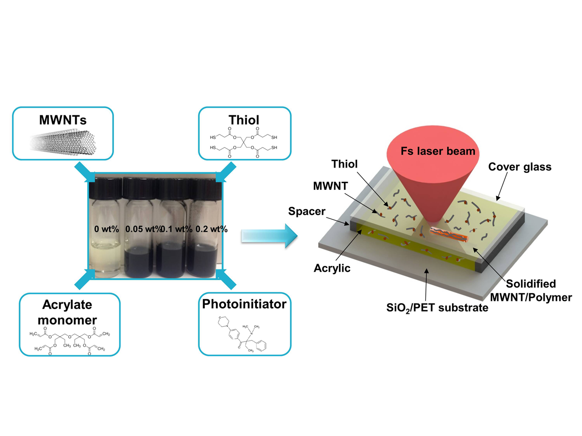
Figure 1. Experimental procedure in preparing CNT-polymer composite resins and the experimental setup of TPP fabrication

CNTs continue to deliver a huge impact on nanotechnology for their remarkable mechanical, electrical, thermal and optical properties. However, it is difficult to achieve both high CNT concentration and homogenous CNT dispersion due to the strong van der Waals interactions among individual CNTs. Moreover, the linear optical absorption of CNTs also limits the maximum doping level of CNTs in composite resins for nonlinear TPP lithography. The relatively low CNT loading concentration leads to limited performance of the composite resins. To overcome these limitations, a TPP-compatible composite material based on multi-walled carbon nanotubes (MWNT), thiol, and acrylic photoresist is presented in here. The schematic illustration of the composite preparation and 3D printing is shown in Fig. 1.

The TPP compatible composite polymer was prepared by directly mixing acrylic monomer, thiol, and photoinitiator with MWNT powder with various weight percentages. The resins prepared showed excellent dispersion of MWNTs through the composite resins and had a high stability last for one week under ambient conditions without obvious MWNT aggregation. Using TPP lithography, a fs laser beam was tightly focused into the composite resin to make 3D scans according to geometric user designs, resulting in solidified 3D micro/nanostructures with MWNTs simultaneously incorporated inside the polymer. After the TPP lithography, the samples were developed with the unsolidified resin rinsed away, leaving the 3D architectures of MWNT-based composite polymer on the substrates. A broad range of functional micro/nanostructures were fabricated, including micro-coil inductor, woodpile, spiral-like photonic crystal, micro-engine inlet fan, micro-car model and micro-gear, as shown in Fig. 2.

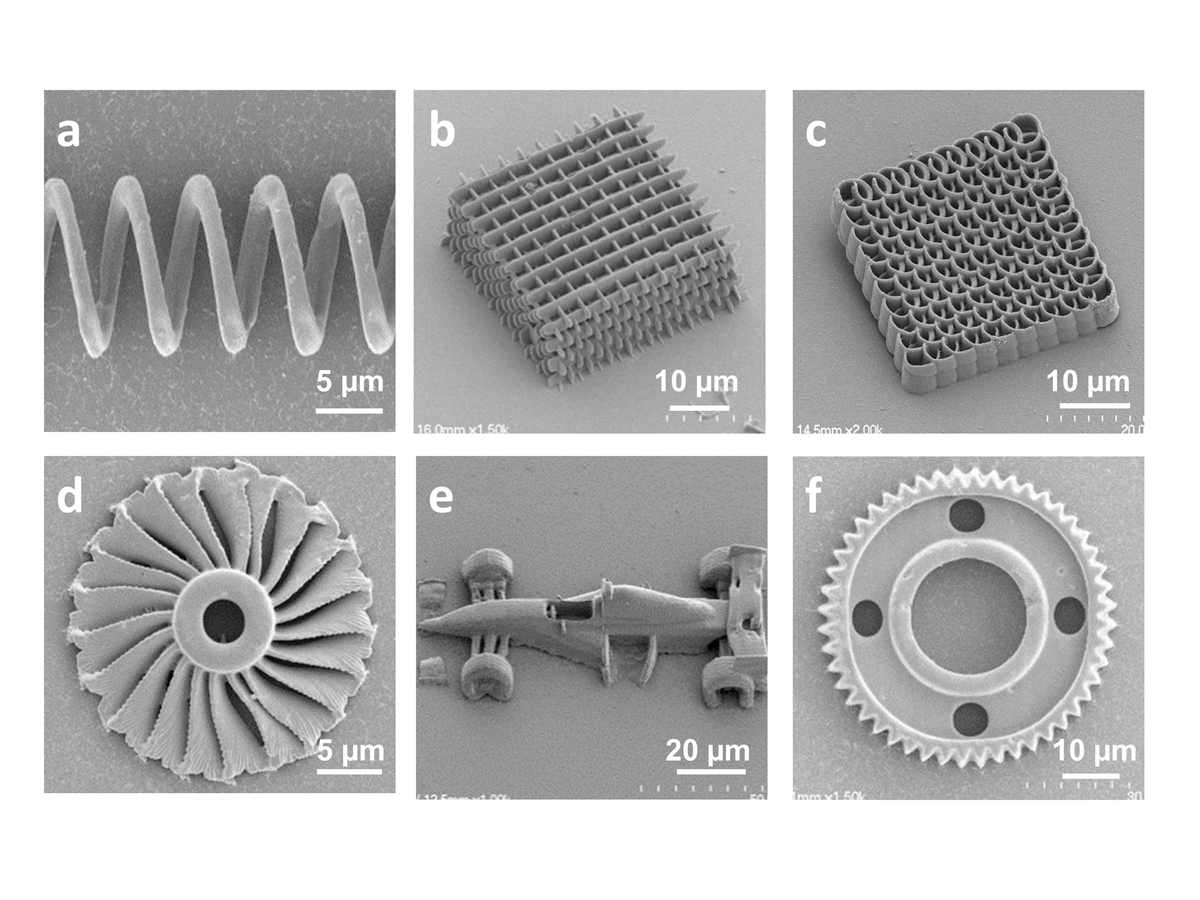
Figure 2. Functional micro/nanostructures fabricated using the MWNT-based composite resins by TPP lithography

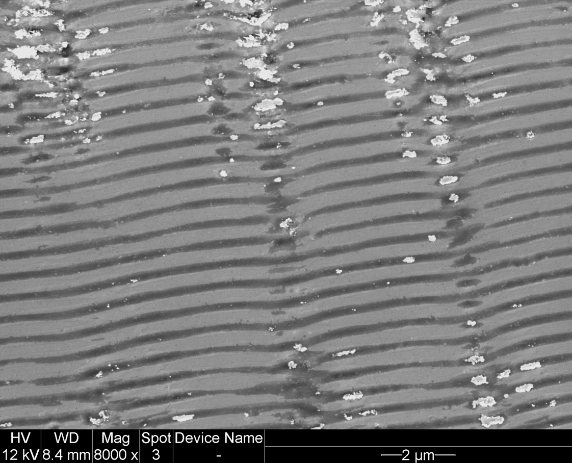
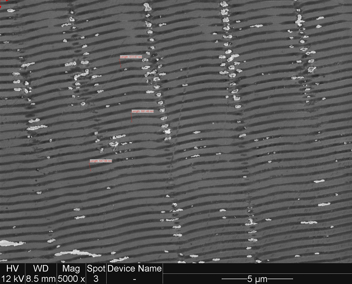
We also studied the distribution and alignment of MWNTs inside the polymer matrix. As shown in Fig. 3, precise assembly of MWNTs was achieved by the combination of TPP fabrication and direct pyrolysis. The length of MWNTs is longer than the laser focal volume, so the trapped MWNTs were forced to align with the laser scan direction. Volume shrinkage can cause tensile strength along the wires, which also contributes to the alignment.

By incorporating MWNTs into the acrylic polymer, the composite resin changed from an insulator to a conductor with greatly enhanced mechanical strength. With 0.2 wt% MWNT concentration, the electrical conductivity of the composite resin increased over 11 orders of magnitude and reached 46.8 S/m, as shown in Fig. 4(a). The superior conductivity of the MTA composite polymers originated from the high MWNT concentration and the uniform MWNT dispersion. Moreover, to utilize the alignment effect of MWNTs in composites, two bar-shaped channels were fabricated with two orthogonal laser scanning directions and showed a three-orders-of-magnitude difference in electrical conductance, which matched with the high anisotropy in electrical conductivity of MWNTs in directions parallel with or perpendicular to the MWNT axis.

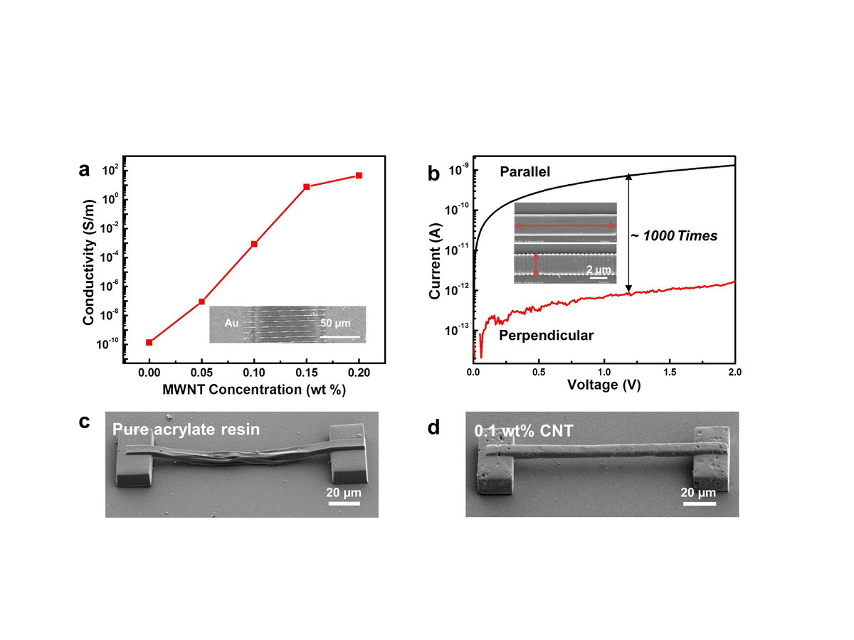
Figure 4. Electrical and mechanical properties of the composite resins

Two suspended microbridges in Fig. 4 (c, d) with the same design were fabricated using the acrylic and composite resins. Under the same fabrication condition, the bridge made by acrylic resin deformed seriously, while the one fabricated by the composite resin remained the straight shape without any obvious deformation, indicating the enhanced mechanical strength by the MWNT loading.
To demonstrate the potential of the composite resins, we fabricated a series of microelectronic devices, including arrays of capacitors (Fig. 5(a)) and resistors (Fig. 5(c)). Fig. 5(b) shows a typical hysteresis loop of a capacitor array containing 10 microcapacitors in parallel. Fig. 5(d) shows the frequency responses of a resistor array containing 20 zigzag microresistors in parallel. The impedance performance of the composite polymer transmission enables its application at high frequency range, such as RF electronics.

Figure 5. MWNT-based functional structures for electronic applications

In summary, a TPP-compatible, homogenous composite resin with high MWNT concentrations has been developed. Various functional 3D micro/nanostructures using the composite resins have been successfully developed via the TPP lithography. Precise MWNT assembly of ~100 nm spatial resolution has been achieved by the combination of TPP lithography and thermal pyrolysis. The composites demonstrated to have increased mechanical strength and enhanced electrical conductivity. 3D printing of micro/nanostructures using highly conductive MWNT-based composites paves the way toward arbitrary precise assembly of MWNTs, which is promising for a broad range of device applications such as 3D electronics and MEMS/NEMS.

Ying Liu is a Ph.D student in Electrical and Computer Engineering at the University of Nebraska-Lincoln. Wei Xiong is a former UNL postdoctoral researcher and is now a professor at Huazhong University of Science and Technology (China). Lijia Jiang is a postdoctoral researcher in electrical and computer engineering at the University of Nebraska-Lincoln. Yunshen Zhou is a research associate professor of electrical and computer engineering at the University of Nebraska-Lincoln. Yongfeng Lu is Lott Distinguished University Professor of engineering at the University of Nebraska-Lincoln.

High Speed Creation of Antireflective Nano Periodic Surfaces via Picosecond Laser Surface Treatment

By: Yung Shin

With the growing need for renewable energy sources, there is an increasing demand for cheap and high-efficiency solar cells. Although high-efficiency silicon solar cells with overall efficiencies higher than 25% [1] have been fabricated in laboratories, the high cost involved in manufacturing these high-efficiency devices makes their commercial use not yet practical. Optical losses through front surface reflections lower the overall efficiency of solar cells since bare silicon reflects nearly 40% of incident solar radiation over the wavelength range of 200 nm to 1100 nm. Anti-reflective coatings have been used to improve solar energy absorption. A more economical alternate solution would be desirable. Texturing the surface of silicon wafers to suppress reflections has been commonly used to improve the efficiency of solar cells [2-5].

Using high-speed, high-power picosecond laser pulse irradiation, low reflectance laser-induced periodic surface structures (LIPSS) could be created on polycrystalline Silicon. A decrease of 35.7% in average reflectance of the silicon wafer was achieved over the wavelength range of 400 nm to 860 nm when it was textured with LIPSS at high scan speeds of 4000 mm/s. A picosecond laser was used to create LIPSS on silicon wafers, which generates linearly polarized pulses with a pulse duration of 10 ps at 532 nm and the focal spot size of 10 µm with a variable repetition rate ranging from 10 KHz to 640 KHz. The period required to achieve the lowest surface reflectance was determined by finite difference time domain (FDTD) simulations, which showed that a period close to 450 nm was the most effective in suppressing reflections in the wavelength range of 200 nm to 1100 nm, which is the range of wavelengths in which silicon solar cells convert light energy to electrical energy. Therefore, the 532 nm wavelength of the laser was chosen with the repetition rate of 640 KHz and a scan speed of 4000 mm/s to create uniform LIPSS over an area of 4 cm by 4 cm. A computer-controlled precision 3-axis stage was used to position the silicon sample under the scanner head. The silicon samples used are 127 mm diameter, 525 µm thick polished wafers. The silicon is N doped with phosphorous and its crystal orientation is (111) with the electrical resistivity less than 0.006 ohm-cm. In order to create LIPSS, the laser was scanned over the surface of the wafer, which was positioned at the focal length of the objective lens. All experiments were conducted with ambient air as the irradiation atmosphere.


Figure 1b. SEM images of highly uniform LIPSS created at a fluence of 0.8 J/cm2 at 8000x magnification

Figure 1a. SEM images of highly uniform LIPSS created at a fluence of 0.8 J/cm2 at 5000x magnification

SEM images revealed that the LIPSS had a period of 532 nm and a fill factor of 75%. The depth of the channels was found to increase with increasing fluence. At 0.8 J/cm2, highly uniform structures were obtained with no surface material removal. The periodic structures appeared to have a flat top surface with filleted edges and deep, narrow valleys. The depth of the valleys was determined through atomic force microscope imaging and was found to range from 150 nm to 350 nm. Fig. 1 shows SEM images of the highly periodic LIPSS created at a fluence of 0.8 J/cm2. At higher fluence values up to 1 J/cm2, the valley depth was found to increase and light was trapped more effectively. At a fluence of 1.1 J/cm2, deep and continuous LIPSS were formed, resulting in an average reflectance of 23.1% corresponding to a 35.7% decrease in average reflectance compared to bare silicon. At even higher fluence values up to 1.2 J/cm2, deep valleys were created with irregularities due to material removal. This resulted in even lower reflectance values due to increased scattering of light below the surface of the material. Beyond this fluence value, the structures no longer appeared periodic. Deep craters and surface irregularities were formed which further enhanced scattering and light trapping below the surface, thus decreasing the average reflectance. Fig. 2 shows the reflectance curves for structures created at different fluence values, across the wavelength range of 400 nm to 860 nm. A clear decreasing trend in reflectance is seen as the fluence is increased. Above this fluence, material removal causes severe damage to the surface.


Figure 2. Reflectance curves showing a decreasing trend in reflectance with increasing fluence values

In order to measure the broadband reflectance of the sample, a Perklin Elmer spectrophotometer was used. First, the sample was checked for opacity, and then the spectral reflectance (R) and transmittance (T) were measured over the wavelength range of 200 nm to 1200 nm. A monochromator was used to resolve the wavelength. Structures made with increasing fluence values exhibited a trend of decreasing average reflectance value. As the fluence was increased from 0.95 J/cm2 to 1.4 J/cm2, the average reflectance over the wavelength range of 400 nm to 860 nm decreased from 25.79% to 19.84%. Fig. 2 shows the reflectance curves for structures created at different fluence values, across the wavelength range of 400 nm to 860 nm. As compared to the reflectance of bare silicon which was measured to be 35.93% over the same wavelength range, a 44.8% decrease in reflectance was achieved for the case of texturing at 1.4 J/cm2. This drop is attributed to the increasing depth of channels and increasing irregularities on the surface.

In summary, silicon wafers with average reflectance values of 23.1% were fabricated by texturing the surface with a picosecond laser. These structures were created at high laser scanning speeds of 4000 mm/s and low pulse overlapping ratios of 60%. Picosecond lasers, due to their lower power density, high rep. rate, and high pulse energy, were shown to be ideal for high-speed surface texturing. With the availability of high-power, high-repetition picosecond laser, the processing speed can further increase, offering the possibility of surface texturing during roll-to-roll manufacturing processes. This method provides an inexpensive and rapid process to create low-reflectance silicon wafers which can be used in photovoltaic applications.

Yung C. Shin is a professor and director at the Center for Laser-based Manufacturing for the School of Mechanical Engineering at Purdue University.

References:
1.) M. A. Green, K. Emery, Y. Hishikawa, W. Warta and E. D. Dunlop, Solar cell efficiency tables (Version 45), Prog. Photovolt: Res. Appl. 2015, 23:1–9
2.) J. I. Gittleman, E. K. Sichel, H. W. Lehmann, and R. Widmer, Textured silicon: A selective absorber for solar thermal conversion, Appl. Phys. Lett. 35, 742 (1979), http://dx.doi.org/10.1063/1.90953
3.) A.W. Smith and A. Rohatgi, A new texturing geometry for producing high efficiency solar cells with no antireflection coatings, Sol. Energ. Mat. Sol. Cells 29 (1993) 51-65
4.)S. Winderbaum, O. Reinhold, F. Yun, Reactive ion etching (RIE) as a method for texturing polycrystalline silicon solar cells, Sol. Energ. Mat. Sol. Cells 46 (1997) 239-248
5.) D.H. Macdonald, A. Cuevas, M.J. Kerr, C. Samundsett, D. Ruby, S. Winderbaum, A. Leo, Texturing industrial multicrystalline silicon solar cells, Sol. Energ. 76 (2004) 277–283

Automated Lasers—The Role of Flexibility

By: Michael Sharpe


FANUC Laser Welding Robot. Image courtesy of FANUC America Corp.

The role of flexibility in supporting the pace of advanced manufacturing through laser innovations is critical for success. Flexibility is essential when designing and building systems to address current and future manufacturing needs. Versatility of core motion control performance, whether in machine or robotic applications, is key to driving the confidence in users and the success of the application. Motion control features for cutting and welding of tomorrow’s products need to build on capabilities which compliments the advances of the past while anticipating unique solutions to meet future functionality. Laser technology demands and deserves progressive and intelligent developments with a strong focus on flexibility and versatility.

Computer Numerical Controls most commonly used on laser processing equipment are mature and readily accepted throughout the industry. Customers have been quite successful at utilizing the full capabilities of laser oscillators when coupled to advanced motion control. At the dawn of NC control and high capacity industrial lasers, manufacturers were mostly using CNC controls in a rectilinear machine. These machines were a simple moving bridge to carry the processing optics in an X, Y plane with Z height control. Rudimentary but they were effective for the application demands of the day.

FANUC high-speed motion control. Image courtesy of FANUC America Corp.

Robots have witnessed recent advancements that have improved motion path performance and I/O trigger accuracy, refining process quality. The downward cost trend of industrial 1μm fiber lasers and increased robotic processing performance has given the industry new vigor, providing the best cost point for high production applications. CNC applications continue to prosper with improved accuracy and speed but are limited in overall flexibility. Customers have more choices than ever based on their manufacturing requirements for laser applications, benefiting all manufacturers of CNC, lasers, and robots.

While it appears straightforward to compare a robot to CNC, they have physical attributes and control nuances that make them each suited for different markets. A laser in motion can produce incredible results but only with the precision of motion control and synchronized input and output control. To effectively use either motion device, it must have the ability to adjust the laser output based on position and velocity. As the motion device accelerates it must have a proportional controlled output to allow the laser power to follow, thereby providing uniform energy distribution along the cut or weld path. Despite their differences, they have similar control functions with different markets. CNC lasers may appear to be more easily deployed as they are mostly configured by machine tool builder in series production, preconfigured for the application purpose. The machines typically offer limited motion range from three degrees of axis motion and up to five degrees in machines with multi-axis heads for orientation control. Most CNCs are rectilinear so they can only do work with one laser processing head at a time, and within their motion envelope. This design cannot support motion overlap of more than one bridge and gantry structure since it will interfere within its own structure. Despite the mechanical design limits, CNCs have enjoyed a large market share in CO2 laser applications as the beam delivery is well suited for the rectilinear structure and its Cartesian motion envelope.

FANUC Robot HiYAG Remote Laser Welding On the Fly. Image courtesy of FANUC America Corp.

The use of CO2 on robots has been limited to specialized applications and was tried early on with some success. The largest problem is beam delivery can become quite complex if not designed properly, though some good solutions exist. Today the robotic CO2 market is primarily plastics trimming where the 10-micron wavelength is more suitable. While fiber delivery is nearly as simple as routing the optical fiber cable along the arm and to the processing head. The cost per watt of a fiber laser has come down significantly while robot motion performance has increased steadily over the last decade and this is where the market has gone in the way of laser processing.

Robot manufacturers continually improve the mechanical structure and motion control to achieve higher path accuracies with improved laser output response. Many features that enhanced the CO2 market are readily available to robot users, including laser height control to adjust the focus, automatic power control to adjust the output to be constant to the travel speed, and laser monitoring. Robotic applications are more flexible because they are not dependent on the rectilinear motion envelope described above. A six-axis robot has the ability to work with other robots and on the same part, improving laser on time. By coordinating or sharing the laser output you can improve efficiency with a smaller investment and with a more compact footprint since the robot takes up only a ‘slice’ of vertical space in the work cell.

FANUC Robot HiYAG Remote Laser Welding. Image courtesy of FANUC America Corp.

Opportunities abound for robotic laser applications and are being largely driven by new materials and construction techniques in the automotive market to the latest in 3D printing technology. The requirements for the latest Café fuel consumption standards and the overweighting of cars with safety equipment has forced manufacturers to seek improvements in materials strength to weight ratio, or light-weighting. Components that are made with hot-pressed steel are more difficult to trim to shape and weld. Fiber lasers offer the flexibility to work in these areas by using the robot to cut and trim hot-stamped components with ease. Robotic fiber laser cutting is a natural extension of the robot’s work envelope or range to process a variety of formed parts that have a 3D profile. Offline programming provides maximum uptime of the laser system, allowing quick changeover since the cutting path can be programmed offline, maximizing valuable laser on time. Path control features allow the robot to self-tune the motion performance to get the most accurate feature. Laser power is controlled through output level, duty, and pulse rate, providing the best cut quality. These functions are automatically adapted to the robot speed, easing the programming.
A popular welding application is remote scanner welding where the beam delivery is controlled by a galvanometer system to steer the beam while coordinating the motion of the robot through its path. This technology is well suited to high throughput applications in automotive body welding and specialty applications for marking and surface treatment. Control techniques to coordinate the robot, scanner, and laser offer precise positioning and are easy to use through a single point of control. Higher throughput is achieved when the robot and scanner’s movements are coordinated with simultaneous control. More nameplate manufacturers are using aluminum for automotive body structures and with class ‘a’ finishes. Complex body shapes have become popular as well as further integration of sensors for safety. The challenge is to form the body shapes and hide the sensors so they do not disrupt the cars’ aesthetics. Wire-fed laser welding solutions help support these initiatives by providing a well-controlled feed rate of filler wire into a body seam while precise laser power control causes the weld to form. All of the welding functions are controlled through the robot and are automatically adapted to the robot tool center point velocity along the weld joint. A high-quality weld is formed without the operator programming special ramping techniques with program outputs, the new adaptive welding systems can handle the welding filler wire and laser power repeatedly.

Aluminum laser welding at a General Motors plant. Image courtesy of
General Motors.

Robotic laser control has matured from the cumulative learning experience of CNC applications while offering the utmost in flexibility. The future looks very bright as more and more laser processes and markets mature such as material conditioning, 3D printing, and future flexible robotic laser applications.

Michael Sharpe is a Staff Engineer in the Materials Joining Group at FANUC America Corp.

High Growth Areas in Industrial Laser Processing & Monitoring

By Craig Bratt & Rahul Patwa

The brilliant light of the laser promises unlimited possibilities for materials processing. Its use in manufacturing dates back to the late 1960s where laser drilling was developed for jet engine components. As laser technology has progressed, fast-paced advances in computers and sensor technologies have enabled the development of improved process monitoring devices which has further enhanced the performance, reliability and ease of use of industrial laser systems.

In 2014, the total global market for laser systems for material processing which include both the source and the components was $9.2 Billion (Source: Optech Consulting, VDMA). From this, the total global laser source revenue was $2.9 Billion, according to the data presented by Industrial Laser Solutions (Feb 2016). In 2015, this revenue (only the global laser source revenue) increased by 6.9% to $3.2 Billion. Although, the largest market share has been and continues to be (61% in 2015) in the laser cutting and laser marking/engraving, their % year-over-year growth has been limited to <5%. More interestingly, the higher % Y-O-Y growth areas are laser welding (17%), laser surface treatment (31%) and laser additive manufacturing (71%).

Courtesy Image

In this article, we present a clear view of how advances in laser power and beam quality along with a significant drop in laser cost per watt and improved laser wall plug efficiency has contributed to major innovations in laser material processing. We have identified four broad laser processing segments and analyzed what is driving innovation.

Manufacturers in many industries have long used laser welding to tackle traditional welding challenges, but laser welding technologies are evolving for even greater utility. Hybrid welding where laser welding is combined with other conventional arc welding methods such as GMAW (MIG) and GTAW (TIG), laser welding with filler wire, and part pre-heating have been successfully implemented in Industry. This has been possible now due to the availability of higher power lasers at lower cost. In turn, materials that were considered difficult to weld until now such as higher carbon steels and cast iron can now be successfully laser welded. The additional filler material changes the composition of the weld, preventing the formation of hard and brittle microstructures. Likewise, induction preheating can be used to help prevent cracking due to martensite formation by slowing down the cooling rate after welding. For instance, in an automotive transmission part, a bolting process was replaced with laser welding, cost savings were achieved through reduced material and processing costs (drilling operations / bolting operations and the bolts themselves), and an overall part weight reduction was accomplished with a more efficient production method using laser technology.

Laser welded transmission part versus traditionally bolted assembly (Courtesy image)

Laser remote welding(Courtesy image)

Remote laser welding is another laser welding process which dramatically reduces welding process cycle times compared to conventional welding and is now possible due to availability of higher beam quality lasers and high speed scanners. It involves the use of moving optics in order to rapidly scan the laser beam across the workpiece over large distances both for high speed and for high precision point to point movement.

To capture the higher potential of laser welding, there has been substantial yet continuous development in laser welding head technology which includes the welding optics themselves and also the sensor optics. Some of these process monitoring technologies have been in development for some time. Some are not yet ready for application at scale. But camera based laser monitoring is now at a point where its greater reliability and lower cost is starting to make sense for high power welding applications.

Fraunhofer CLA has developed a high speed camera vision system which can record the welding process in high clarity in real-time and provide both image and video data from the process. This information is processed and calibrated with reference data based on pre-determined actual ‘good’ weld measurements using reinforcement learning. Using customized image processing software algorithms, it is possible to detect many of the most common weld defects.

One laser processing technology which has recently been moving up to forefront of innovative, or even disruptive technologies is laser additive manufacturing (LAM). This process uses laser beam as heat source and is primarily divided in two processes: Selective laser melting (SLM) and Laser metal deposition (LMD).

In the SLM process, a layer of powder is deposited on a build platform and then a rapidly scanned laser beam fuses powder together in the right shape and multiple thin powder layers are deposited to create complex 3D parts.

Fraunhofer Coax wire deposition head allows multi directional build up using wire. (Courtesy image)

In the LMD process (also known as direct energy deposition or laser cladding), the laser is used to melt metal powder fed through the nozzle which is then deposited in layers onto a substrate, which results in a full metallurgical bond with a small heat affected zone and minimal dilution. It has been developed for surface wear and corrosion coatings, component repairs/remanufacturing, and generation of complete components from scratch.

Fraunhofer process monitoring system hardware (Courtesy image)

Two other variations of LMD—hot/cold wire cladding and internal diameter cladding—have now evolved into successful industrial processes and are now widely used in the oil industry, agriculture, power generation and remanufacturing sectors. A recent key development by Fraunhofer IWS is a new coax laser deposition head COAXwireTM which provides
omni-directional welding performance for the use of metallic wires as filler material which is of particular use for 3D build up additive manufacturing of metallic components.

One area of laser material processing that has benefitted the most from technology improvements in both spatial and temporal properties of the laser is laser machining. In addition, the advent of lower cost and smaller footprint laser power sources has lead to much wider industrial adoption of laser technology. The latest generation of pulsed lasers with pulse lengths—from millisecond all the way to femtosecond—has led to a rich pipeline of innovations impacting virtually every manufacturing industry. For example, laser cutting of battery electrodes can produce excellent cut quality and achieve high cutting speeds for application in lithium-ion battery cell production. Similarly lasers can be used for coating removal for electrical contacts on battery foils. Large area coating removal for paint stripping, deoxidization, mold and die cleaning or removal of special coatings is conducted by applying high power lasers. Lasers are also used for high rate drilling process for up to 15,000 holes/second.

Fraunhofer high speed camera system software (Courtesy image)

In summary, the current pace of innovations leading to new laser technologies and products is constantly increasing with a wide array of new applications being developed for every industry imaginable.

Craig Bratt, Executive Director, Fraunhofer USA, Center for Laser Applications, cbratt@fraunhofer.org

Rahul Patwa, Project Manager, Fraunhofer USA, Center for Laser Applications, rpatwa@fraunhofer.org

Approaching Photonic Serial Production: Laser-remote-processing of Automotive CFRP Components

By: Dr.-Ing. Peter Jaeschke, Laser Zentrum Hannover e.V.

The efficient use of limited resources is one of the greatest challenges of our times. To address this, lightweight solutions and concepts are already being adapted for the transportation industry, in particular within the automotive and aerospace sectors. However, in order to broaden the use of lightweight materials, there needs to be suitable processing, testing and measuring techniques in place for a variety of materials, constituting a prerequisite for economic, flexible and automated high volume production. In this context, photonic technologies can provide solutions. Since the operating mode of the laser is both highly flexible as well as no-contact, and thus wear-free, it offers numerous benefits for the machining materials, especially as an alternative to conventional processing methods encumbered by high tool wear. Furthermore, the energy input, tailored to the respective manufacturing requirements, offers new possibilities for the processing of temperature-sensitive materials.

In the supporting measures “Photonic Processes and Tools for Resource-Efficient Lightweight Construction” within the framework of the program “Photonics Research Germany“, the German Federal Ministry of Education and Research (BMBF) is aiming at overcoming existing constraints regarding the wide use of lightweight materials in serial production. For the corresponding R&D activities, the BMBF is providing a total amount of approx. 30 Mio. €. The initiative “Photonic Processes and Tools for Resource-Efficient Lightweight Construction“ is coordinated by Laser Zentrum Hannover e.V., Hannover, Germany (Figure 1).

Figure 1. The German initiative “Photonic Processes and Tools for Resource-Efficient Lightweight Construction“ is supported by the Federal Ministry of Education and Research and co-ordinated by Laser Zentrum Hannover e.V. (Source: LZH)

Within this research initiative, nine co-operative projects under industrial leadership are working on the development of laser sources and optical components as well as system technology and applications. In addition to welding and the surface preparation for both metallic parts and hybrid materials, the laser based processing of composites, particularly continuous carbon and glass fiber reinforced plastics forms the core issues of the BMBF initiative.

In this context, the main R&D activities focus on composite processing. This is comprised of cutting and drilling RTM parts, robotically-guided 3-D scanning optics and CFRP reparation preparation using short pulsed laser radiation. Other examples include composite surface preparation for adhesive applications, direct bonding, and joining of metal-metal interfaces as well as composite-metal hybrids. In the field of laser material processing, continuous carbon fiber reinforced plastic (CFRP) based parts and components represent a relatively new material class, exhibiting outstanding mechanical properties at a low density. As a result, such composites have been identified to have significant potential in lightweight construction for a wide variety of industrial applications.

During the manufacturing process of CFRP parts, trimming, drilling and ablation steps are of particular importance. Another point is the layer-by-layer removal to prepare the repair or rework of defects. In this context, conventional machining techniques, such as milling, drilling, grinding or abrasive waterjet cutting, which are well developed for a wide variety of industrially established materials, suffer from high tool wear, insufficient quality or their complex setup and limited flexibility when it comes to the requirements of CFRP machining.

The main reason for this is the heterogeneous composition of CFRP. Combining both carbon fibers, either arranged as fabrics or non-crimped fabrics, with a polymer matrix, either thermoset or thermoplastic, produces a unified material with very different individual material properties, and as results presenting a very unique challenge from a material processing perspective. Furthermore, for cutting applications both components have to be processed simultaneously which causes enormous difficulties. In this regard, the processing of CFRP components brings many challenges.

Photonic processes, however, offer solutions for many of these: Including the high flexibility and, in particular, the contactless, wear-free mechanism of the laser that offers advantages for the processing of CFRP materials. For the processing of complex components or temperature-sensitive materials, the locally limited and to the given manufacturing requirements adjusted energy input offers new opportunities. An implementation of laser-based processes in serial production in industry, however, requires a thorough understanding of the process, a high degree of automation as well as the consideration of environmental and occupational safety aspects.

If CFRP is processed with NIR lasers, carbon fibers show excellent optical absorption and heat dissipation, contrary to the plastics matrix. Therefore heat dissipation away from the laser focus into the material is driven by heat conduction of the fibers. The matrix is heated indirectly by heat transfer from the fibers. To cut CFRP, it is required to reach the melting temperature for thermoplastic matrix materials or the disintegration temperature for thermoset systems as well as the sublimation temperature of the reinforcing fibers simultaneously. One solution for this problem is to use short pulse nanosecond lasers, as has been demonstrated in one of the joint research projects, HolQueSt3D.

Figure 2. Towards serial production: Laser-Remote-Processing of automotive CFRP components (Source: LZH).

Based on an existing lightweight part used in the automotive industry, LZH has developed remote cutting processes for three-dimensional composite structures (Figure 2). A newly developed high-power disc laser of the TRUMPF Laser GmbH serves as the basic process technology. This fiber-guided laser source emits at 1030 nm and is providing a maximum average output power of 1.5 kW. With a constant pulse length of 30 ns, the maximum pulse energy of 80 mJ is realized for a repetition rate of 18.8 kHz. For remote processing of the automotive part, the KMS Automation GmbH has designed a clamping system, custom designed to address the specific requirements of laser processing of CFRP components. One of these requirements is an integrated exhaust system for the process emissions. The impact of laser processing on the characteristics of the components as well as on possible subsequent processes, e.g. primer and painting steps, has been investigated by the partners Volkswagen AG and INVENT GmbH.

Another priority was the development of repair concepts for 2D and 3D components. For this purpose, the LZH developed process strategies for the scarfing of defective areas. Due to the flexible system technology, it is possible to remove large areas on complex free-form surfaces. After the laser based repair preparation, the TU Clausthal developed repair concepts that work without hardening in autoclaves, making a more flexible and cost-efficient repair possible.

Furthermore the detection and analysis of the process emissions as well as the development of a catalytic exhaust air treatment system matching the requirements of laser-based CFRP processing played an important role. Based on the emission measurement during the processing, the Jenoptik Automatisierungstechnik GmbH has developed a fully regenerative, continuously working exhaust air cleaning system. As the involved end user, the Volkswagen AG supported the development of the process during the whole duration of the project, and evaluated its suitability for serial production. By processing an existing component used in automotive industry, the suitability of the developed processes was proven at the end of the project.

The supporting measures “Photonic Processes and Tools for Resource-Efficient Lightweight Construction“ within the framework of the program ”Photonics Research Germany“ is funded by the German Federal Ministry of Education and Research (BMBF). The author would like to express his gratitude to the corresponding overall project management VDI Technologiezentrum GmbH for their support. Furthermore the author would like to thank all coordinators of the involved co-operative research projects for their engagement and their support of the co-ordination work as well as all partners of the HolQueSt3D-project for their excellent work in a constructive manner.