TRUMPF to Showcase Latest Laser Technology Advancements & Products at Photonics West 2022

FARMINGTON, Conn., January 21, 2022 – In booth 327 at Photonics West 2022, TRUMPF Inc. will showcase its TruMicro 2000 Series, TruMicro 6000 Series, TruFiber P Compact, and TruMark Station 7000 laser marking station with a TruMark 6030 laser marking system and VisionLine 3 feature recognition capability. TRUMPF will also display two Tool Bars highlighting its wide range of laser technology offerings and VCSEL laser diode technologies as part of its exhibit at the Moscone Center in San Francisco, California.

New Glass Processing Optics for TruMicro Lasers


The TruMicro 2000 series laser is equipped with two of the latest innovations in optics for beam formation when cutting and welding glass: TOP Cleave and TOP Weld. TOP Cleave optics enable quick laser cutting of glass parts with excellent edge quality and nearly eliminates necessary post processing. TOP Weld makes it possible to weld glass with a top layer as thick as 8mm and also weld both glass to glass and glass to metal. TOP Weld can create a tight, hermetic seal to keep liquids and gases in or out. Both optics work with the fiber-based ultrashort pulse lasers in the TruMicro Series 2000, distinguished by its compact and light design. TruMicro Series 2000 solid-state lasers are tailored for precision micro-processing with an optimal combination of quality, productivity, and profitability.

The TruMicro 6330 ultrafast industrial laser also cuts glass and can separate flexible printed circuit boards. Designed for batch production in consumer electronics and other industries, the TruMicro 6330 is ideally suited for high-speed scanning applications such as cutting polymer stacks and processing OLED displays. Notable for strong performance, stability and quality, the ultrashort pulse lasers of the TruMicro Series 6000 generate laser pulses that can be linearly amplified to very high pulse energies.

TruFiber 200 P Compact

One of TRUMPF’s compact, fiber-based solid-state lasers, the TruFiber 200 P Compact will also be shown. This robust fiber laser resonator has a compact footprint, long service life, and patented technology that protects the laser from the damaging effects of back-reflected light, enabling it to process materials, such as copper, brass or gold, easily and productively. TruFiber P Compact lasers are suitable for a variety of applications including additive manufacturing and precision laser cutting and welding.

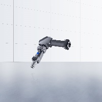
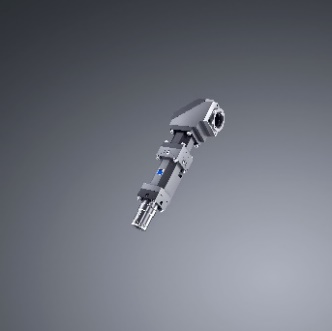
Laser Marking Station with TruMark 6030 and VisionLine 3

At the show, TRUMPF will be demonstrating a TruMark Station 7000 laser marking station featuring a TruMark 6030 laser marking system and VisionLine 3 feature recognition capability. The TruMark 6030 is a high-performance marking laser with 3D functionality. The laser’s outstanding beam quality and high power densities ensure clean material removal and high-contrast markings. The TruMark 6030 can be integrated quickly and easily into production systems and can reduce process time by up to 25 percent through its available high average power and pulse energy at the workpiece. The VisionLine 3 camera-based image processing product creates an additional level of safety during processing. VisionLine 3 automatically detects component positions before welding and aligns each job accordingly.

Also on Display: VCSEL and Other Laser Technology


The booth will also showcase TRUMPF’s wide range of other laser technology offerings, including the VCSEL laser diode technologies of TRUMPF Photonic Components. TRUMPF Photonic Components is a global technology leader supplying state-of-the-art VCSEL and photodiode solutions for the consumer electronics, datacom, industrial sensing and heating markets. Experts anticipate this growing market will drive the future of mobile electronics, autonomous driving, optical data communication, and quantum technology.

TRUMPF will be located at booth 327 in the Moscone Center in San Francisco, California. Press kits will be available at the booth.


About TRUMPF

TRUMPF is a high-tech company offering manufacturing solutions in the fields of machine tools and laser technology. The Company drives digital connectivity in the manufacturing through consulting, platform products and software. TRUMPF is a technology and market leader in highly versatile machine tools for sheet metal processing and in the field of industrial lasers. In 2020/21, the company employed 15,000 people and generated sales of about 3.5 billion euros. With over 80 subsidiaries, the TRUMPF Group is represented in nearly every European country as well as in North America, South America and Asia. The company has production facilities in Germany, France, the United Kingdom, Italy, Austria, Switzerland, Poland, the Czech Republic, the United States, Mexico and China.

Find out more about TRUMPF at www.trumpf.com

Discover the Benefits of Public-Private Partnerships in Additive Manufacturing with America Makes at LAM 2018

Our Laser Additive Manufacturing (LAM®) Conference is less than 2 months away. This annual event features a series of presentations from industry leaders that highlight the latest advancements in additive manufacturing technology, applications, policy, standards and training for a variety of industries.

LAM 2018 is in Schaumburg, Illinois, and will be co-located with the Lasers in Manufacturing Event (LME). All LAM attendees will be granted free access to the LME exhibit and reception at the end of the sessions on the second day.

This year’s event will kick off with the keynote presentation “Smart Collaboration: A Public-Private Approach to Advancing the Manufacturing Industry” by America Makes, as part of the Policy and Technology I session. Learn more about America Makes’ work and the keynote speech at LAM below.


America Makes Helps Improve the U.S. Economy Through Domestic Manufacturing

America Makes at the 2017 NAMII Announcement Event

The National Center for Defense Manufacturing and Machining (NCDMM) manages and operates America Makes, the National Additive Manufacturing Innovation Institute, which is a public-private partnership focused on research and innovation in additive manufacturing and 3D printing. America Makes is comprised of member organizations from industry, academia, government, non-government agencies, and workforce and economic development resources. The NCDMM is a nonprofit organization dedicated to improving America’s workforce and economic competitiveness through the development of new manufacturing solutions.


What’s Next for America Makes

March 5th through March 9th, America Makes will offer the first public Advanced Curriculum in Additive Design, Engineering and Manufacturing Innovation (ACADEMI) course, Metals Design for Additive Manufacturing, for both its members and non-members. The course will cover advanced design with a focus on new areas of design spaces, engineering, manufacturing, and processing techniques for additive manufacturing with metallic materials.

On March 6th, America Makes will also host a free public forum on their Apprenticeship Works Program to promote manufacturing apprenticeships and introduce the first-ever, industry-vetted Additive Manufacturing (AM)/3D Printing Technician Registered Apprenticeship framework. This new framework serves to help employers develop registered apprenticeship programs within their companies to help employees advance their skill sets.

For more information, visit https://www.americamakes.us.

Do not miss the America Makes presentation, “Smart Collaboration: A Public-Private Approach to Advancing the Additive Manufacturing Industry” on March 27, 2018 at 8:15 AM as part of the LAM opening session, Policy and Technology I. For more information on this year’s sessions and presentations, please visit: https://www.lia.org/conferences/lam/program.


Laser Additive Manufacturing Workshop (LAM) will take place March 27-28, 2018 in Schaumburg, Illinois. For more information, and to register, please visit www.lia.org/lam.

The Laser Institute of America (LIA) is the international society for laser applications and safety. Our mission is to foster lasers, laser applications, and laser safety worldwide. Visit us for conference, education, and courses information at http://www.lia.org today.


Laser Institute of America Presents Additive Manufacturing: Trends in North America Session at World of Photonics Congress 2017

As part of the World of Photonics Congress’s Additive Manufacturing subconference at LiM 2017, North American laser manufacturing leaders shared a comprehensive look at the latest developments and innovations.

ORLANDO, FL – The Laser Institute of America (LIA) presented its 90 minute session,  AM: Trends in North America, on Wednesday, June 28, 2017 at the International Congress Center in Munich, Germany. The session was part of the Additive Manufacturing subconference of Lasers in Manufacturing (LiM) 2017 at the World of Photonics Congress Lasers in Manufacturing event, held from June 26-29, 2017 and organized by the German Scientific Laser Society (WLT).

The session was part of the Additive Manufacturing subconference of Lasers in Manufacturing (LiM) 2017 at the World of Photonics Congress Lasers in Manufacturing event.

Lasers in Manufacturing (LiM) is a scientific conference focusing on the latest trends in laser materials processing for industrial applications. LiM prides itself as a comprehensive international forum for researchers and experts in laser-based manufacturing.

World of Photonics Congress meets biannually, uniting the “scientific elite” to gather information in the realm of photonics research. The event covers all aspects of research from application-based topics, to the latest applications in industry and medicine. World of Photonics Congress also offers conferences and practice-oriented application panels.

LIA shares in the World of Photonics Congress’s mission of providing laser professionals with valuable events that present and discuss innovative insights with the laser community. The new 90-minute session specifically focused on North American additive manufacturing bolstered the body of knowledge in industry research at the global LiM gathering.

“LIA was honored to collaborate with World of Photonics Congress on this year’s inaugural North American additive manufacturing event,” said Jim Naugle, LIA’s Marketing Director. “We are excited to add our insight and knowledge to the collective expertise found at LiM and are thrilled about this year’s robust attendance. Due to its success, we look forward to possibly expanding our role at future events.”

Attendees enjoyed the unique perspective on the success of North American AM regarding cost and increased efficiency. Keynote speaker David Ott of the Global Humanitarian Lab (GHL)

Attendees enjoyed the unique perspective on the success of North American AM regarding cost and increased efficiency.

discussed 3D printing’s impact on humanitarian efforts in the private, academic, and scientific sectors, while addressing communities affected by disasters globally. Author Rob Martinsen, CTO of nLight, presented breaking solutions in AM. Additional featured speakers included author William Herbert, Director of Corporate Development for Carpenter Technologies, and Yannick Lafue, Business Developer for Aeronautics Defense and Oil & Gas at IREPA LASER.

The World of Photonics Congress included sessions on macro processing, micro processing, additive manufacturing, as well as award ceremonies, lectures and specialty technology sessions.

For more information on upcoming LIA events and conferences, including ICALEO 2017 and LAM/LME 2018, visit https://www.lia.org/conferences.

###

About LIA

The Laser Institute of America (LIA) is the professional society for laser applications and safety serving the industrial, educational, medical, research and government communities throughout the world since 1968. http://www.lia.org, 13501 Ingenuity Drive, Ste 128, Orlando, FL 32826, +1.407.380.1553.

Diode Lasers in Cladding, Additive and Hybrid Manufacturing

By Oleg Raykis

Today there exist a number of technologies for additive manufacturing of components.

The two most prominent types utilizing lasers for generating parts out of metals are either powder bed based solutions or direct energy deposition, often referred to as laser metal deposition. As a company Laserline focuses mainly on the second type. Depending on the application it allows you to produce larger part sizes with higher productivity (deposition rates and therefore higher productivity) due to the fact of not being limited by the size of the building chamber as it would be in the case of a powder bed machine. It is also much faster in many cases.

Laserline identified four main application areas for AM in which we operate and be described based on examples in this article. Those areas include, besides generating complete parts by terms of additive manufacturing, also repair welding application or hybrid machines – a combination of conventional machining and laser technology the fourth main application area would be providing functional areas on conventionally manufactured parts.

Additive manufacturing technology allows generating shapes and structures in a single production step with little material loss, post machining and tool wear (near-net-shape manufacturing). Thereby you can use material in powder or wire form. The advantage of using wire is that you will have a 100% material utilization; the compromise on the other hand might be the directional dependency when you supply the wire laterally and not coaxial. Pic. 1 shows an example of a free form application as a rocket nozzle demonstrator part made out of Inconel 625.

Pic.1 Free form powder AM of a rocket nozzle demonstrator (Source: Fraunhofer CLA)

The part was done without any type of process control. Another interesting example of AM with Titanium is shown in Pic.2.

Pic. 2 Ti64 powder AM with closed loop process control (Source: Fraunhofer CLA)

Compared to the rocket nozzle, process control was used when producing the demonstrator part in pic.2. The camera based system (in this case E-MAqS) is capable of measuring the size and temperature of the melt pool. Furthermore it can give feedback to the laser source and adjust the laser power accordingly to maintain the desired size of the melt pool. This in turn ensures consistent reproducible part build ups with no defects.

Another very interesting and promising approach is to integrate the laser source into machine tools. There are several hybrid machine tool concepts being developed; one of them is the combination of additive and subtractive tools which achieves a new level of manufacturing. One example is the merger of a laser with a 5-axis milling machine. The integrated diode laser deposits the powdered metal layer by layer, generating a solid, fully dense metal part. The following milling operations directly finish machines surfaces in areas necessary, without changing setup.

Pic.3 An example of a conventional milling machine with integrated AM technology (Source: DMG Mori-Seiki)

This flexible switch between laser and mill also allows the machining finish of areas, which would be impossible to reach on the final component. Designs with undercuts, internal geometries and overhangs without support structure are no problem. The manufacturing of completely new structures and designs are now possible. All weldable metals, which are available in powder form, can be used, for example steel, nickel and cobalt alloys as well as titanium, bronze or brass.

A third important field of AM from our perspective are repair welding applications. Probably the most prominent and widely industrially utilized are the repairs of turbine blades. Turbine blades in steam engines, especially in the first two rows, experience a lot of wear through erosion. Instead of replacing the whole part it is possible to repair the worn area by putting a couple of layers (mostly nickel / cobalt based super alloys) and machine them down to the finished surface, see Pic.4.

Pic.4 Turbine blade repair (Source: Fraunhofer ILT)

This remanufacturing procedure saves up to 90% of material and energy cost compared to manufacturing a new blade. Even though turbine blades are the most prominent example of laser repair welding a wide variety of other parts can be restored using the procedure, e.g. worm shafts, helical gears, molds, etc. to name a few. When speaking about additive manufacturing most people have the production of complete parts in mind. This doesn’t always have to be the case. Often it makes more sense from an economic standpoint to add to a conventionally (and relatively inexpensively) produced part functional areas where they are needed. Pic. 5 shows one such example.

Pic. 5 Extruder barrel demonstrator (Source: Fraunhofer CLA)

In this case 100 lbs. of hard and wear resistant Stellite 21 powder material was deposited on a metal pipe base structure to form the extruder thread. One further example of it can be functional layers on drill bits where sensors need to be shielded from magnetic interference. By creating heat resistant layers out of non-magnetic materials it is possible to place those sensors.Through a clever combination of the usage of conventional and additive manufacturing technologies it is possible to produce advanced parts without increasing the cost.

Quality Assurance of Selective Laser Melting Applications

By Thomas Gruenberger

Key differentiation criteria for Additive Manufacturing (AM) technologies are freedom of design, cost advantage, customization, and time to market.

Direct metal laser sintering (DMLS) AM technology is ideal for serial production for industries like aerospace.

Setting up a process means mapping the input parameters (e.g. machine and process parameters and part geometry) to output parameters (part properties like density, tightness, surface quality). An in-situ nondestructive measurement of part properties like density is not possible, so indirect measurements have to be performed. Information from the process – process emissions, melt pool size, melt pool dynamics, and temperature distribution – can be used for this indirect measurement enabling the user to find a correlation between features of these measurements and the resulting part properties. Additionally, a shorter process development time can be achieved by avoiding destructive tests during development learning reading the extracted features (see Fig. 1).

Fig. 1: Quality inspection – the challenge

As mentioned above, several pieces of information from the process can be used for the detection of irregularities, so different sensor technologies can be used. Consider a manual in-situ inspection of the process, where the user looks at the visible process emissions in the process chamber. Differences in brightness, size, color, and number of sparkles can be detected with the human eye. This can be automated using photodiode based meltpool monitoring systems like the plasmo fast process observer, a hardware developed by plasmo with up to 4 channels at sampling rates up to 300kHz.

So the system measures the brightness of the process emissions over time (blue curve in Fig. 2), using CAD data, the data can be mapped easily to an image of brightness of process emissions over the building platform (see Fig. 2 right plot), layer for layer, in pseudo color representation.

Fig. 2: Feature map of the building process

Running an OK process gives the baseline of the feature, provoking process irregularities yields in a change of the feature, enabling the user to set limits for the feature according to its quality needs. A pseudo color representation of a map of process irregularities can be calculated, giving the user an easy way to understand visualization and therefore, fast feedback about the quality of the process. As a note, black means no process irregularities and yellow means 100 percent of process irregularities in the given pixel in Fig. 3.

Fig. 3: Map of process irregularities

The fully automated measurement system enables a 100 percent inspection of the building process. The high sampling rate (ca. 10,000 times fa

ster compared to the human eye) enables the system not only to calculate features like signal height but the additional analysis in time, frequency and time scale domain can be performed, too. Three (3) different algorithms (features) are calculated by the system and each algorithm can be parametrized according to the quality needs for every exposure type used in the layer.

These algorithms are easy to explain. Based on physics, they correspond directly to process different phenomena.

  • Absolute limits: Influences in the size and form of the cross section of one exposure like focal position, laser power and welding speed
  • Signal dynamics: Noisy processes or less process dynamics like pollution, protective gas flow and lack of fusion
  • Short time fluctuations: Short changes in the signal caused by e.g. ejects and pollution

In cooperation with EOS, the described system was integrated with their machines. A typical layout is shown in Fig. 4.

Fig. 4: System layout – EOSTATE Meltpool

As shown in Fig. 4, two total photodiodes are used an onAxis diode measuring the process emissions at the interaction zone of the laser beam and powder and an offAxis diode giving an overview of process emissions about the complete building platform.

A heuristic model is used for setting up the system; therefore, input parameters like process parameters (laser power, scanning speed, gas flow, …) and malfunctions like loss of laser power, and material quality are varied for different building jobs. The output parameters are part properties (porosity, surface roughness, …), process emissions (brightness, temporal behavior, spectral properties, …) and undesired effects like overheating, warpage and lack of fusion. Based on this data set the system can be parametrized to fulfill the quality needs of the customer.

Fig. 5 shows a provoked malfunction, missing powder choosing a too low dosing factor of powder, the irregularities (here red in Fig. 5) can be easily detected.

Fig. 5: Example missing powder, left image of powder bed, right calculated irregularities after exposure

Fig. 6 shows a phenomena process flipping provoked by changing the focal position, the irregularities (red in Fig. 6) can be detected successfully for the complete parts and also the embedded parts (letter F).

Fig. 6: Example process flipping, left image of building platform after complete build, right calculated irregularities

Successful detection of additional phenomena has been shown:

  • Overhanging parts
  • Dust/particles
  • Part overlap
  • Balling / humping
  • SLI pores (simulated porosity)
  • To be continued.

The presented diode based meltpool monitoring system enables the fully automated detection of process phenomena (see Fig. 7) which directly corresponds to part properties.

Fig. 7: Example stable and unstable process, top image of process emissions, middle measured brightness, bottom windowed FFT analysis

Easily understandable algorithms based on physics are applied and can be parametrized by the user according to its needs. A heuristic model for setting up limits was presented and examples of detectable process phenomena are given. The system is part of an integrated quality inspection portfolio at EOS including EOSTATE powderbed and EOSTATE system monitoring.

Further investigations in detectable process phenomena and self-healing effects of defects will be completed. Additional work is in progress in the field of statistical data processing, so information (see Fig. 8, e.g. trends, …) is extracted from data visualized in dashboards enabling the user to perform statistical process control (SPC) at one machine up to different machines at different locations worldwide.

Fig. 8: Statistical process control

About plasmo 

Headquartered in Vienna, Austria, plasmo is an innovative, globally operating technology company for automated quality assurance systems in manufacturing industries. Established in 2003, plasmo leads the way in the real-time quality control of joining processes. The extensive portfolio in the field of quality assurance includes laser power measurement, the monitoring of welding processes, geometric shapes and surfaces, tailor-made solutions in the field of industrial image processing, analysis software as well as an extensive range of services.

With over 700 plasmo systems in operation worldwide, the growing list of clients includes ABB, Benteler, BorgWarner, Faurecia, INA, SMS Siemag, Hettich, JCI, Magna and Valeo to Webasto, and numerous automobile manufacturers such as Audi, BMW, Daimler, Ford, GM, PSA, Suzuki, Volvo as well as various international steel manufacturers. www.plasmo-us.com

© 2017 Dr. Thomas Grünberger, plasmo Industrietechnik GmbH, Vienna