Following the trend of additive manufacturing methods, such as 3D printing, the utilization of 3D scanning for measurement is on the rise.
According to a new report by MarketsandMarkets, the market for 3D scanners is expected to grow to nearly six billion dollars by 2020, a significant increase from 2015’s $3.41 billion. A compound annual growth rate of 9.6 percent is also projected.
The public summary of the report suggests that the growth is driven by new developments in 3D scanner technology, the capacity for quality control with the devices, and the time saved by stronger quality control.
Laser-based 3D scanners are expected to take up the majority of the market share. This figure includes devices that use laser triangulation, phase shifting, time of flight, or a combination of all three as “laser 3D scanners.”
The Leica Absolute Scanner LAS-20-8. (Image courtesy of Hexagon MI.)
The report also reveals that the market is significantly concentrated in the Americas, followed closely by Asia and other Pacific regions, due to rising applications in fields such as automotive, healthcare, and construction industries.
The full report can be found through MarketsandMarkets here.
By Wilhelm Pfleging, Melanie Mangang, Yijing Zheng, Peter Smyrek and Johannes Pröll
Introduction
Thick film anodes and cathodes with thicknesses ranging from 20-300 µm, in state-of-the-art and future lithium-ion cells are complex multi-material systems consisting of defined material components, grain sizes, porosities and pore size distributions in the micrometer and submicrometer ranges. State-of-the-art cells with pouch cell geometry for high power applications consist of thick film electrode stacks with capacities up to 40-50 Ah.
The development of three-dimensional (3D) cell architectures for electrodes in lithium-ion batteries is a promising approach to overcome problems like 1-dimensional lithium-ion diffusion, inhomogeneous current densities, power losses, high interelectrode ohmic resistances as well as mechanical stresses due to high volume changes resulting from lithium-ion insertion and deinsertion. By applying 3D battery architectures, one can achieve large areal energy capacities while maintaining high power densities at the same time. This feature is important, e.g., for thin film batteries where the lithium-ion diffusion is limited by the thickness of the compact film. A common approach for realization of 3D architectures in electrodes is the structuring of the substrate or current collector. An increased active surface achieved by 3D electrode architectures can induce large areal energy densities. Unfortunately, this approach is in a very early stage of development and in general it is not feasible for state-of-the-art electrodes.
Figure1. Laser-generated self-organized microstructure in composited electrode cathode material
At the Karlsruhe Institute of Technology (KIT), a new process for the generation of 3D electrode designs has been created by developing two processes; 1.) Laser-assisted self-organized structuring (Fig. 1) and 2.) direct structuring of tape cast electrodes [1-3].
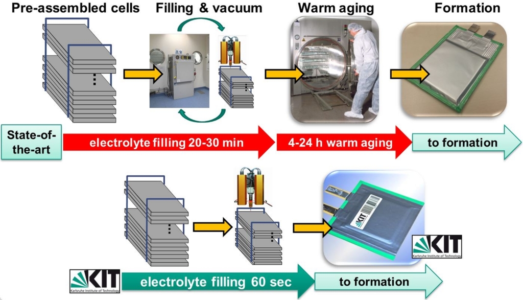
In each case, the laser structured electrodes exhibit a significant improvement in liquid electrolyte wetting as well as in electrochemical performance after laser treatment. During the manufacturing process of lithium-ion cells, liquid electrolyte filling is a cost- and time-consuming process. Insufficient electrolyte wetting in turn can lead to unexpected cell failure under challenging cycling conditions. At KIT, a cost efficient laser-based technology for the realization of 3D architectures in thick-film tape-cast electrodes was developed to accelerate the wetting process and to also shorten the time-span for cell manufacturing (Fig. 2).
Figure2. State-of-the-art processing route for liquid electrolyte filling of lithium-ion cells with time-consuming warm aging (top) and KIT process without warm aging due to laser structured battery materials (bottom)
In addition, an improved cell operation with extended life-time and increased capacity retention at high charging and discharging currents could be achieved. For the development of advanced laser processes in battery manufacturing, a complete lithium-ion cell manufacturing process cycle has been built-up which includes electrochemical characterization of lithium-ion cells (Fig. 3).
Figure 3. Process chain for cell fabrication and testing including laser processing of battery materials
Experimental Setup
Different types of electrode materials were already investigated such as LiCoO2 (LCO), LiMn2O4 (LMO), SnO2 (SnO), fluorine doped SnO2 (FTO), Li(NiMnCo)O2 (NMC), silicon (Si), graphite (C) and LiFePO4 (LFP). Thin films as well as thick films were applied. Thick film electrodes are composite materials which consist of active material, carbon black, graphite and binder. All lithium-ion cells were assembled either in an argon-filled glove box or in a dry room. An ultrafast fiber laser system (Tangerine, Amplitude Systèmes, France), a ns fiber laser system (YLPM, IPG Photonics, Germany), or an excimer laser system (ATLEX-1000-I, ATL Lasertechnik GmbH, Germany) were used to manufacture 3D architectures into the thin or thick film electrode layers.
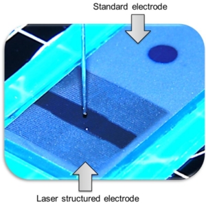
Figure 4. Rapid wetting of laser structured electrodes
The Results
In general, electrolyte filling of lithium-ion cells is realized by time and cost consuming vacuum and storage processes at elevated temperatures. Nevertheless, by applying state-of-the-art electrolyte filling processes, insufficient wetting of electrode and separators is one drawback resulting in a certain production failure rate accompanied with a lowered cell capacity or a reduced cell life-time. Laser structuring has been developed for the formation of capillary micro-structures in thick film tape-cast electrodes which resulted in the acceleration of electrolyte wetting in comparison to unstructured electrodes (Fig. 4). The removal of the complete electrode material from the ablation zone delivers the most efficient capillary transport [4].
For the formation of capillary structures, ns-laser ablation as well as ultrafast laser processing was investigated.
For ns-laser radiation (l=1064 nm, pulse length 200 ns) the laser beam energy is absorbed at the material surface and, due to heat conduction, the temperature of the surrounding composite material increases. The binder material for tape-cast electrodes (~5 wt%) is PVDF which has a low decomposition temperature in the range of 250–350° C [5]. Therefore, the PVDF binder matrix spontaneously evaporates and active particles are removed from the laser beam interaction zone.
Figure 5. Capillary structures in NMC electrodes. Cross section and SEM top view of ns- (a & b) and fs- (c & d) laser structured NMC (pitch of capillary structures: 200 µm, pulse lengths: 200 ns, 350 fs)
With ns-laser radiation, structure widths of about 40-55 µm can be achieved (Fig. 5a & 5b). The current collector for cathodes are made of aluminium with a thickness of 20 µm and for anodes they consist of copper with a thickness of 10 µm. Laser structuring with a ns-laser can be realized without damage of the current collector (Fig. 5a). Laser structuring can be realized even for double-side coated aluminium substrates, which is a required processing step for process up-scale for manufacturing of lithium-ion cells with high capacities [4].
Nanosecond laser ablation is not appropriate for each type of electrode material. For example, ns laser structuring of LFP electrodes always leads to melt formation and therefore to an undesired modification of the active material. Furthermore, the ablation efficiency of LFP increases by a factor of 3 by using femto- or pico-second laser ablation in comparison to ns-laser ablation [6]. Another aspect is the loss of active material due to the ablation process. For the application of structured foils in batteries, it is important to reduce the amount of ablated material which in turn means that small capillary widths and high aspect ratios are preferred. By using ultrafast laser ablation it could be shown that the aspect ratio could be significantly increased (Fig. 5c & 5d) and that the loss of active material can be reduced from 20 percent down to values below 5 percent [7].
Capacity retention and cell life-time can be illustrated by plotting the cell voltage as function of discharge capacity for different cycle numbers. For the lithium-ion cell with the structured NMC electrode, the 80 percent capacity limit of the initial discharge capacity is reached after 2290 cycles (Fig. 6). While the cell life-time for the lithium-ion cell with unstructured electrodes is reached after 141 cycles. Furthermore, the discharge capacity of the cell with the laser-structured NMC electrode reaches a value of 108 mAh/g after 2290 cycles indicating that efficient liquid electrolyte transport due to micro capillary structures improves the electrochemical performance for cell without cost- and time-consuming storage procedures.
Figure 6. Cell voltage versus discharge capacity for pouch cells with laser-structured (right) and unstructured (left) NMC electrodes and without storage [4]
Summary & Conclusion
A new technical approach of using laser-generated capillary structures in electrode materials was presented. This technology can be applied in order to increase cell reliability during the production process, to shorten production times of lithium-ion cells as well as to increase the cell life-time during cycling. Due to an improved cycle life-time and increased capacity retention, the use of high power batteries in 2nd life applications becomes interesting. Cost-efficient ns fiber lasers can be applied for carrying out the structuring process for several types of electrode materials. Nevertheless, regarding the structuring of LFP, a further reduction of active mass loss, and an up-scaling of the structuring process, the use of ultrafast laser processing becomes necessary.
References
J. Pröll, H. Kim, A. Piqué, H.J. Seifert, W. Pfleging, J. Power Sources, 255(0) (2014), 116-124.
J.H. Park, R. Kohler, W. Pfleging, W. Choi, H.J. Seifert, J.K. Lee, RSC Adv., 4(9) (2014), 4247-4252.
R. Kohler, J. Pröll, M. Bruns, S. Ulrich, H.J. Seifert, W. Pfleging, Appl. Phys. A, 112(1) (2013), 77-85.
W. Pfleging, J. Pröll, J. Mater Chem A, 2(36) (2014), 14918-14926.
J. Choi, E. Morikawa, S. Ducharme, P.A. Dowben, Mater Lett, 59(28) (2005), 3599-3603.
M. Mangang, H.J. Seifert, W. Pfleging, J. Power Sources, 304 (2016), 24-32.
P. Smyrek, J. Pröll, H.J. Seifert, W. Pfleging, J. Electrochem Soc, 163(2) (2016), A19-A26.
Wilhelm Pfleging, Yijing Zheng, Peter Smyrek and Johannes Pröll are all with the Karlsruhe Nano Micro Facility in , Germany. They are joined by Melanie Mangang in their work at Karlsruhe Institute of Technology (KIT).
When it comes to space travel, getting from point A to point B, at a faster rate is among the biggest challenges facing researchers, eager to explore new worlds. One researcher, however, thinks that he has found a solution that could reduce travel time to Mars to less than one hour, using laser-based technology.
The process, known as directed energy propulsion, involves focusing a laser on small spacecraft, speeding it up to a fraction of the speed of light. In doing so, trips to nearby systems can be potentially fractionalized, taking hours rather than months to reach a destination. This could all be possible thanks to the research of Phillip Lubin, a scientist working with NASA’s Innovative Advanced Concepts Program.
According to Lubin’s research, space travel via directed energy propulsion would require a small, “wafer-thin” spacecraft. The spacecraft would be equipped with a laser sail, just over three feet long called DE-STAR (Directed Energy System for Targeting of Asteroids and ExploRation.) A strong laser in Earth’s orbit would be fired at the sail, accelerating it into space.
The small size of the spacecraft (around 200 lbs) would not make directed energy propulsion an option for manned travel or heavy cargo. However, equipping the craft with simple instruments as a way to collect data in “fly-by” missions is something it is more than capable of. Another concern for the concept is the fact that without an equal laser at the opposite end of where the craft is headed, it would not stop. While this does limit the capabilities of the craft, using it almost exclusively as a research tool opens up the door for future, similar developments. Rather than relying on rocket fuel, accelerating through chemical propulsion, using light to obtain lightspeeds uses electromagnetic acceleration, in a fraction of the time. Lubin expands on this in the paper A Roadmap To Interstellar Flight, which details the research that earned Lubin and his team a proof-of-concept grant from NASA.
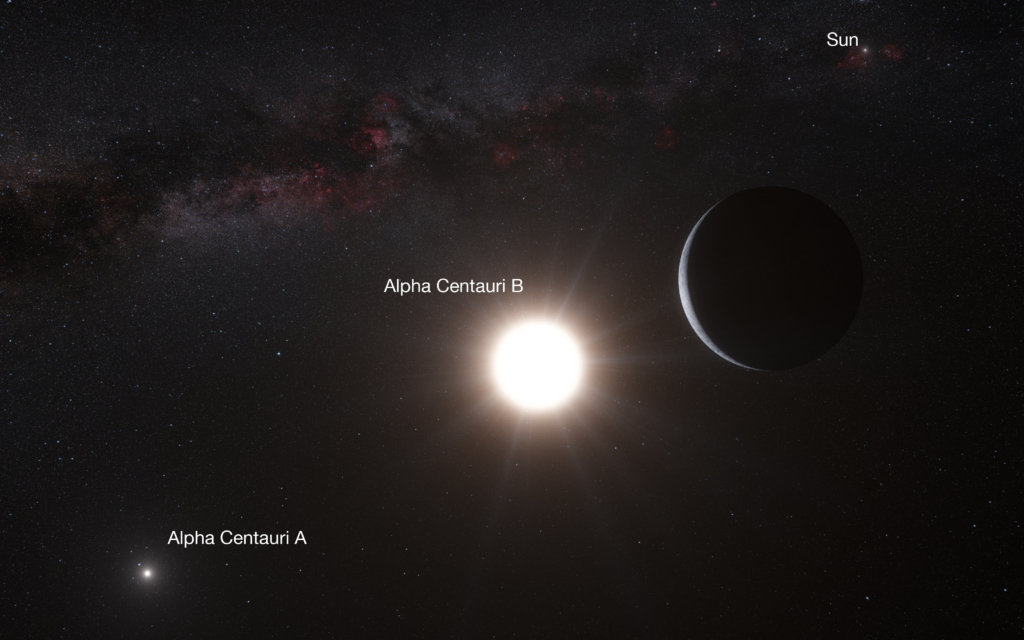
Should NASA greenlight direct energy propulsion for space travel, the proposed spacecraft could potentially expand past our neighboring planets and into nearby star systems, like Alpha Centauri. The speed made possible by directed energy propulsion could cut down the travel time to the star system, located approximately four light years away, to less than 20 years. “There is no known reason why we cannot do this,” Lubin says in “Going Interstellar,” a NASA 360 video, detailing the concept.
While shooting lasers at a spacecraft, headed toward Mars sounds like a science fiction concept, it is very much rooted in what is possible today. As the application of laser-based technologies becomes more commonplace in utilization, LIA continues to foster lasers and laser safety worldwide. For information on laser safety training and more, please visit www.lia.org
If you have ever been to Auckland, New Zealand, you know the natural beauty of its surroundings and the vibrancy of the city. What you may not know is that the campus of the University of Auckland is home to a unique facility, one that uses the power of intense pulses of light to manipulate, measure and machine matter — it uses photons as its ‘machinery.’
The Photon Factory
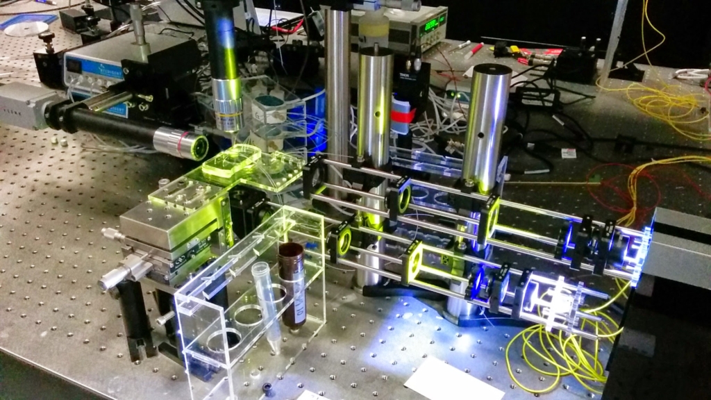
This unexpected find is the result of the efforts of Dr. Cather Simpson, who joined the faculty of the University of Auckland in 2007. Soon after arriving, Dr. Simpson challenged herself to “bring the rich versatility of high-tech ultrashort laser pulses to New Zealand academic and industry innovators.” This challenge resulted in the creation of a facility dubbed the ‘Photon Factory.’ The Photon Factory fulfills multiple functions: it is a laboratory for education, research, innovation and even economic development.
The ‘Photon Factory’ at the University of Auckland (left) and Dr. Cather Simpson (right) along with members of her team of students, researchers & entrepreneurs
Dr. Simpson became familiar with ultrafast lasers and their extremely short pulses (on the order of 100 fs = 100 x 1015 seconds) while pursuing research in ultrafast energy conversion in molecules. She used them as a tool in her lab when she started her career as a professor at Case Western Reserve University (CWRU). Light can be converted by molecules into other forms of energy; by studying the dynamics of molecular complexes excited by light on femtosecond to microsecond timescales through both experiments and modeling, it is possible to learn how molecules direct the energy acquired in light absorption. The ultimate goal of these investigations is to understand how the structure and environment influence molecular functions so that photochemical and photophysical behavior can be both predicted and tailored.
Having achieved tenure at CWRU, she found the opportunity to move to New Zealand compelling, and there, her research has flourished to span from fundamental spectroscopy to applied device development. The Photon Factory is the facility and resource she has developed to accomplish her research goals and to bring the power of laser light to New Zealand, and beyond.
A Factory of Ideas & People, Powered by Light
How did the Photon Factory come into being? When Dr. Simpson moved to New Zealand, the country was undergoing a transformation in how academic research was being funded. A newly-formed government was in the process of making structural changes, closing the Ministry of Research, Science and Technology and moving some of its functions to a newly created agency, the Ministry of Business Innovation and Employment. This signaled the new government’s stance that science and technology were to be viewed as drivers of economic development. Because she arrived at this time and had no history with the previous methods of funding, Simpson was able to embrace and navigate the new system. She realized that the government wanted to use the academic community to fill a large gap in R&D spending that New Zealand companies were not filling — the level of spending on internal R&D was well below that of international companies, and nearly non-existent. She also realized that, unlike what she had encountered in America, funding sources would scrutinize how she engaged with industry and what type of business case there was for the proposed work as a key factor in whether her work would be funded or not. She began to pay attention to what companies were identifying as the problems they wanted to solve. But at the same time, she was eager to continue her ultrafast chemistry research.
Dr. Simpson recognized that the laser tools that she was using in chemistry were being used for other applications, some that might have more immediate use to industry. Her experience and interest in laser-matter interactions was a natural bridge into material processing applications. She also understood that there were challenges, such as slow machining speeds, that kept ultrashort pulsed machining from widespread use. With these ideas in mind, the multi-purpose, multi-user Photon Factory, was born.
Since its opening in 2010, the facility has grown to over 30 students and employees from physics, chemistry and engineering backgrounds who work on dozens of academic and commercial projects. These activities range from basic research stemming from Simpson’s chemistry background, such as evaluating the photobehavior of improved solar energy harvesting molecules, to more industry-friendly applied research, such as fabricating photomasks for microfluidic chip production.
The Photon Factory generates commercial contracts and grants, and also serves as a test bed for science innovation and a training ground for future scientists and engineers. Interactions with New Zealand-based companies including Next Window, Rakon, Fisher & Paykel, Izon and others have produced such wide-ranging results as improved touch-sensitive displays, better locking nuts, more efficient designs for solar thermal energy harvesting, and new designs for GPS chips. Global companies like Intuitive Surgical (based in Sunnyvale, CA) have brought projects to the Photon Factory to develop laser-based surgery in difficult tissue. Such projects have yielded patent filings, and an increased ability to understand commercial opportunities. They have also created conditions for both students and Dr. Simpson herself to get involved in industry-sponsored and spin-off technologies.
Entrepreneurship has become a buzzword in academic circles, but in New Zealand, the Photon Factory takes the concept to heart. Two spin-off companies have already been generated by the work of the Photon Factory. The first, Engender Technologies, Ltd., was established in 2011 as a result of taking a serious look at the challenges faced by New Zealand’s dairy industry. When approached by a venture capital firm with the five top problems in that sector, Dr. Simpson found one that seemed possible to address by photonics and then chose a team of students and engineers to find a solution. The problem she chose was that of improving sperm sorting by sex, to address the needs of dairy farmers who are turning to artificial insemination to control the numbers of bulls versus cows. The resulting microfluidic and photonic device is a huge departure from the state-of-the-art flow cytometry based solution, and one that could only be identified by people with a new set of tools at their disposal. A second spin-off is currently being formed to commercialize a new centrifugal microfluidic technology developed in the Photon Factory to analyze milk at “point of cow” in the milking shed. The new company already has backing from VC and other investors. It is probably no coincidence that both start-ups are addressing New Zealand’s important agricultural sector.
Cell-sorting prototype developed within the Photon Factory
Transforming Matter & Lives
So, what has the Photon Factory achieved thus far? Besides new chemical insights, material processing to solve diverse problems, and generating novel concepts and devices, it has turned Dr. Simpson into an entrepreneur and led her to tackle questions that she previously would not have envisioned. Her passion for research has been applied to significant problems in diverse application areas, from touch sensor displays to challenges in dairy farming. And perhaps most importantly, this passion has been applied to developing future engineers and scientists with deep curiosity and an entrepreneurial spirit. All of these things have resulted from the fortuitous confluence of a researcher, with a specialized high-tech tool, finding interesting challenges and opportunities based on New Zealand’s desire to develop more innovation to drive economic growth. Who knew that photons could be so powerful?
For more information, or to reach Dr. Cather Simpson, visit www.photonfactory.auckland.ac.nz/en.html
Researchers at Arizona State University have created white laser light with an array of semiconductor lasers in a compact arrangement. The project helps pave the way toward better lighting and light-based wireless communication, as white lasers are more luminous and energy efficient than LEDs.
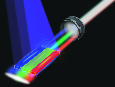
This schematic illustrates the novel nanosheet with three parallel segments created by the researchers, each supporting laser action in one of three elementary colors. The device is capable of lasing in any visible color, completely tunable from red, green to blue, or any color in between. When the total field is collected, a white color emerges. Photo by: ASU/Nature Nanotechnology
ASU researchers created a novel nanosheet — a thin layer of semiconductor that measures roughly one-fifth of the thickness of human hair in size and roughly one-thousandth the thickness of human hair — with three parallel segments, each supporting laser action in one of three elementary colors. The device is capable of lasing in any visible color, completely tunable from red, green to blue or any color in between. When the total field is collected, a white color emerges.
The advance puts lasers a step closer to being a mainstream light source and potential replacement or alternative to light emitting diodes. Lasers are brighter, more energy efficient, and can potentially provide more accurate and vivid colors for displays like computer screens and televisions. Ning’s group has already shown that their structures could cover as much as 70 percent more colors than the current display industry standard.
Another important application could be in visible light communication in which the same room lighting systems could be used for illumination and communication. The technology under development is called Li-Fi for light-based wireless communication, as opposed to the more prevailing Wi-Fi using radio waves. Li-Fi could be more than 10 times faster than current Wi-Fi, and white laser Li-Fi could be 10 to 100 times faster than LED based Li-Fi under development.
“The concept of white lasers first seems counterintuitive because the light from a typical laser contains exactly one color, a specific wavelength of the electromagnetic spectrum, rather than a broad-range of different wavelengths,” Ning explained. “White light is typically viewed as a complete mixture of all of the wavelengths of the visible spectrum.”
Sandia National Labs in 2011 produced high-quality white light from four large lasers. The researchers showed that the human eye is as comfortable with white light generated by diode lasers as with that produced by LEDs, inspiring others to advance the technology.
But “those independent lasers cannot be used for room lighting or in displays,” Ning said. “A single tiny piece of semiconductor material emitting laser light in all colors or in white is desired.”
Semiconductors, usually a solid chemical element or compound arranged into crystals, are widely used for computer chips or for light generation in telecommunication systems. They are used to make lasers and LEDs because they can emit light of a specific color when a voltage is applied to them. The most preferred light emitting material for semiconductors is indium gallium nitride, though other materials such as cadmium sulfide and cadmium selenide also are used for emitting visible colors.
The main challenge lies in the way light emitting semiconductor materials are grown and how they emit light of different colors. Typically a semiconductor emits light of a single color — blue, green or red — that is determined by a unique atomic structure and energy bandgap.
The “lattice constant” represents the distance between the atoms. To produce all possible wavelengths in the visible spectral range you need several semiconductors of different lattice constants and energy bandgaps.
“Our goal is to achieve a single semiconductor piece capable of laser operation in the three fundamental lasing colors. The piece should be small enough so that people can perceive only one overall mixed color instead of three individual colors,” said Fan. — Sharon Keeler, chief media officer, Ira A. Fulton Schools of Engineering. Read more about the research here.


![Figure 6. Cell voltage versus discharge capacity for pouch cells with laser-structured (right) and unstructured (left) NMC electrodes and without storage [4]](https://www.laserstoday.com/wp-content/uploads/2016/04/Fig-6-1024x400.jpg)