In 2018, Laser Institute of America (LIA) will commemorate its 50th year as a professional society dedicated to fostering lasers, laser safety and applications. In 1968, the company was founded by a passionate group of academics consisting of scientists, developers, and engineers who desired to turn the emerging laser world into a valuable and practical industry.
LIA has always believed in the importance of developing a culture of innovation, ingenuity and inspiration within the laser industry. As a professional society, it serves industrial, educational, medical, research and governmental communities internationally.
“We are very excited to launch into LIA’s 50th anniversary,” said Nat Quick, LIA’s executive director. “We want to celebrate this significant milestone and take the opportunity to reintroduce LIA as the face of laser safety and applications.”
In its anniversary year, LIA will update its brand with a new logo and new look for its print and electronic newsletters. Additionally, the association is introducing exclusive LIA gear with the release of its 50th-anniversary pins and shirts.
LIA TODAY, its bi-monthly, full-color print magazine that publishes articles on the latest industry news, will be revamped. Readers can expect a new look for both the print magazine and LIA’s monthly eNewsletter. The new overall appearance will be modernized and consistent with the look and feel of LIA’s newly launched website.
“Our team is looking forward to refreshing the LIA brand,” said Jim Naugle, LIA’s marketing director. “Additionally, we have a number of events planned commemorating advances in laser technology, our history and our valued LIA members.”
LIA has scheduled four conferences/exhibits in 2018 — LAM, LME, Industrial Laser Conference and ICALEO. Special events will take place at each of the conferences/exhibits. Details will be announced on event pages and upcoming issues of LIA TODAY.
With so much to look forward to in the coming year, the company as a whole is grateful to the laser community for its consistent support and contribution. To learn more about LIA and its upcoming celebrations, visit www.lia.org/50years.
As the LIA team reflects on the last five decades, they will develop a timeline marking significant industry-related benchmarks. Once established, this timeline will be available digitally and at conferences throughout the year. You are encouraged to contribute notable events and achievements. For submission details, visit www.lia.org/50years/timeline.
As a leader and pioneer in developing and commercializing fiber lasers, IPG Photonics’ diverse lines of low, medium, and high-power lasers and amplifiers are displacing traditional technologies in many current applications. Their lasers and amplifiers reach into numerous markets, including materials processing, communications, entertainment, medicine, and biotechnology.
Founded in Russia in 1991 by physicist Valentin P. Gapontsev, Ph.D., IPG originally produced and sold customized glass and crystal lasers, laser components, and wireless temperature meters for hyperthermia. In 1992, the company began to focus on the development of high-power fiber lasers and amplifiers.
IPG landed its first major contract with Itatel, a telecommunications carrier. The company then won a second major contract with DaimlerBenz Aerospace. In 1994, IPG opened a facility in Germany and established its world headquarters in the U.S. in 1998. In 2000, the company invested in new high-capacity production facilities in the U.S. to manufacture its own diode pumps—a major component of its fiber lasers and amplifiers. The company went public in 2006 and is listed on the NASDAQ Global Select Market as IPGP.
With more than 4,000 employees today, IPG has local sales and service in more than 20 countries worldwide. Its three major manufacturing sites are currently located in the U.S., Germany, and Russia.
IPG’s vertically integrated development and manufacturing abilities allow the company to meet customer requirements, accelerate development, manage costs, and improve yields. The company is able to produce all critical components for its lasers and amplifiers, which it markets to OEMs, system integrators, and end users.
Being the first company to industrialize fiber laser technology, IPG has the broadest array of laser products in the industry. This includes high-power fiber lasers up to 100 kW for materials processing, pulsed fiber lasers for marking and engraving, and fiber lasers covering UV, visible, and mid-IR wavelengths.
Having displaced the traditional CO2 and diode-pumped solid-state technologies as the preferred laser tool for industrial material processing, IPG’s high-power CW fiber laser product line is arguably the most important offered by the company. These lasers are used in the cutting, welding, and drilling of metals within various industries ranging from automotive to aerospace to general manufacturing. Much of this product line’s success can be attributed to IPG’s in-house diode fabrication facility, which accounts for cost reductions.
In the next five years, IPG is looking toward the introduction of cost-effective, high-performance, reliable ultra-fast fiber lasers with a pulse duration in the 100 fsec to 10 psec range. With a higher efficiency, this laser advancement will enable smaller air-cooled packages. The company is also looking toward the expansion of fiber laser technology into the MID-IR wavelengths.
The improved reliability and increased efficiency of high-fiber power lasers as an accepted mainstream industrial tool has led to increase in laser adoption in the automotive industry, a trend that is expected to continue with the push to adopt lightweight materials and electric or battery-driven cars. IPG has monitored these shifts in the industry and will continue to be a leading developer in this area.
IPG Photonics has been a member of LIA since 2002. For more information about the company and its products, visit www.ipgphotonics.com.
This was written by Lindsay Weaver Burt in collaboration with IPG Photonics.
Advanced three-dimensional (3D) micro/nanofabrication of functional devices represents a key research topic in modern nanoscience and technology and is critically important to numerous scientific and industrial applications. Among various existing 3D micro/nanofabrication methods, two-photon polymerization (TPP) based on laser direct writing is regarded as one of the most promising methods due to its unique combination of true three dimensionality and high spatial resolution.
The TPP technique is based on the nonlinear interaction of femtosecond laser pulses with photosensitive material, which induces a highly localized chemical reaction leading to polymerization of the photoresist with current resolutions down to 40 nm. The capability of the TPP technique is significantly determined by the properties of photoresists employed, which are electronic insulating in general. To increase the functionality and expand the applications of TPP, we used carbon nanotubes (CNT) as filling materials in the host polymers.
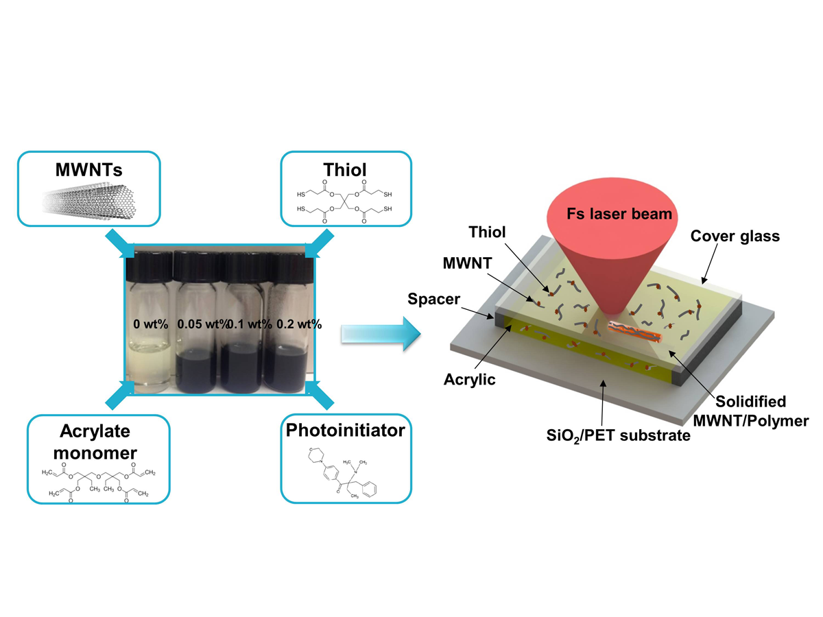
Figure 1. Experimental procedure in preparing CNT-polymer composite resins and the experimental setup of TPP fabrication
CNTs continue to deliver a huge impact on nanotechnology for their remarkable mechanical, electrical, thermal and optical properties. However, it is difficult to achieve both high CNT concentration and homogenous CNT dispersion due to the strong van der Waals interactions among individual CNTs. Moreover, the linear optical absorption of CNTs also limits the maximum doping level of CNTs in composite resins for nonlinear TPP lithography. The relatively low CNT loading concentration leads to limited performance of the composite resins. To overcome these limitations, a TPP-compatible composite material based on multi-walled carbon nanotubes (MWNT), thiol, and acrylic photoresist is presented in here. The schematic illustration of the composite preparation and 3D printing is shown in Fig. 1.
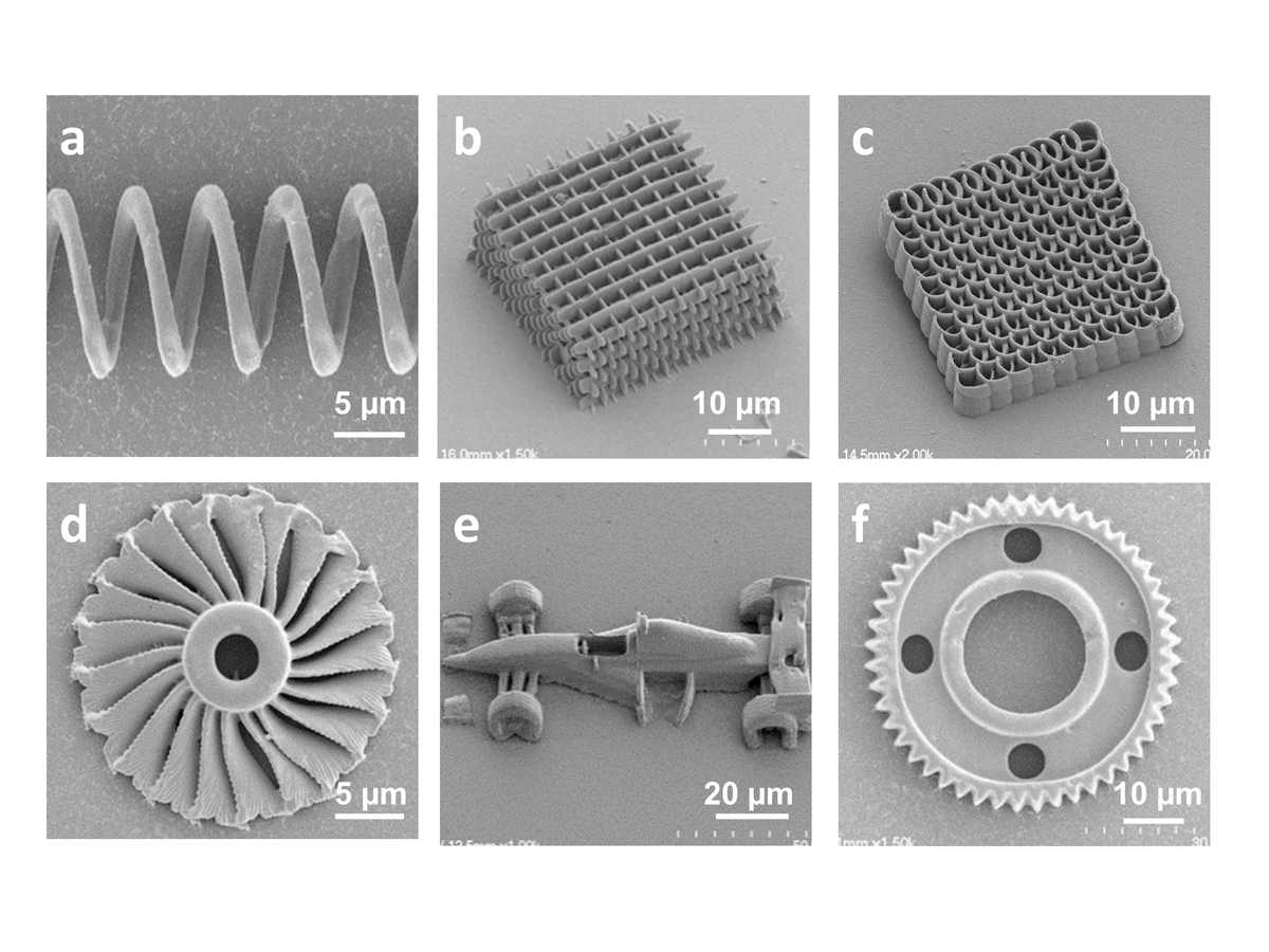
The TPP compatible composite polymer was prepared by directly mixing acrylic monomer, thiol, and photoinitiator with MWNT powder with various weight percentages. The resins prepared showed excellent dispersion of MWNTs through the composite resins and had a high stability last for one week under ambient conditions without obvious MWNT aggregation. Using TPP lithography, a fs laser beam was tightly focused into the composite resin to make 3D scans according to geometric user designs, resulting in solidified 3D micro/nanostructures with MWNTs simultaneously incorporated inside the polymer. After the TPP lithography, the samples were developed with the unsolidified resin rinsed away, leaving the 3D architectures of MWNT-based composite polymer on the substrates. A broad range of functional micro/nanostructures were fabricated, including micro-coil inductor, woodpile, spiral-like photonic crystal, micro-engine inlet fan, micro-car model and micro-gear, as shown in Fig. 2.
Figure 2. Functional micro/nanostructures fabricated using the MWNT-based composite resins by TPP lithography
We also studied the distribution and alignment of MWNTs inside the polymer matrix. As shown in Fig. 3, precise assembly of MWNTs was achieved by the combination of TPP fabrication and direct pyrolysis. The length of MWNTs is longer than the laser focal volume, so the trapped MWNTs were forced to align with the laser scan direction. Volume shrinkage can cause tensile strength along the wires, which also contributes to the alignment.
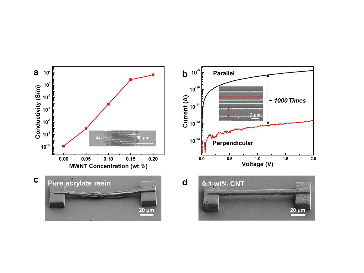
By incorporating MWNTs into the acrylic polymer, the composite resin changed from an insulator to a conductor with greatly enhanced mechanical strength. With 0.2 wt% MWNT concentration, the electrical conductivity of the composite resin increased over 11 orders of magnitude and reached 46.8 S/m, as shown in Fig. 4(a). The superior conductivity of the MTA composite polymers originated from the high MWNT concentration and the uniform MWNT dispersion. Moreover, to utilize the alignment effect of MWNTs in composites, two bar-shaped channels were fabricated with two orthogonal laser scanning directions and showed a three-orders-of-magnitude difference in electrical conductance, which matched with the high anisotropy in electrical conductivity of MWNTs in directions parallel with or perpendicular to the MWNT axis.
Figure 4. Electrical and mechanical properties of the composite resins
Two suspended microbridges in Fig. 4 (c, d) with the same design were fabricated using the acrylic and composite resins. Under the same fabrication condition, the bridge made by acrylic resin deformed seriously, while the one fabricated by the composite resin remained the straight shape without any obvious deformation, indicating the enhanced mechanical strength by the MWNT loading.
To demonstrate the potential of the composite resins, we fabricated a series of microelectronic devices, including arrays of capacitors (Fig. 5(a)) and resistors (Fig. 5(c)). Fig. 5(b) shows a typical hysteresis loop of a capacitor array containing 10 microcapacitors in parallel. Fig. 5(d) shows the frequency responses of a resistor array containing 20 zigzag microresistors in parallel. The impedance performance of the composite polymer transmission enables its application at high frequency range, such as RF electronics.
Figure 5. MWNT-based functional structures for electronic applications
In summary, a TPP-compatible, homogenous composite resin with high MWNT concentrations has been developed. Various functional 3D micro/nanostructures using the composite resins have been successfully developed via the TPP lithography. Precise MWNT assembly of ~100 nm spatial resolution has been achieved by the combination of TPP lithography and thermal pyrolysis. The composites demonstrated to have increased mechanical strength and enhanced electrical conductivity. 3D printing of micro/nanostructures using highly conductive MWNT-based composites paves the way toward arbitrary precise assembly of MWNTs, which is promising for a broad range of device applications such as 3D electronics and MEMS/NEMS.
Ying Liu is a Ph.D student in Electrical and Computer Engineering at the University of Nebraska-Lincoln. Wei Xiong is a former UNL postdoctoral researcher and is now a professor at Huazhong University of Science and Technology (China). Lijia Jiang is a postdoctoral researcher in electrical and computer engineering at the University of Nebraska-Lincoln. Yunshen Zhou is a research associate professor of electrical and computer engineering at the University of Nebraska-Lincoln. Yongfeng Lu is Lott Distinguished University Professor of engineering at the University of Nebraska-Lincoln.
With the growing need for renewable energy sources, there is an increasing demand for cheap and high-efficiency solar cells. Although high-efficiency silicon solar cells with overall efficiencies higher than 25% [1] have been fabricated in laboratories, the high cost involved in manufacturing these high-efficiency devices makes their commercial use not yet practical. Optical losses through front surface reflections lower the overall efficiency of solar cells since bare silicon reflects nearly 40% of incident solar radiation over the wavelength range of 200 nm to 1100 nm. Anti-reflective coatings have been used to improve solar energy absorption. A more economical alternate solution would be desirable. Texturing the surface of silicon wafers to suppress reflections has been commonly used to improve the efficiency of solar cells [2-5].
Using high-speed, high-power picosecond laser pulse irradiation, low reflectance laser-induced periodic surface structures (LIPSS) could be created on polycrystalline Silicon. A decrease of 35.7% in average reflectance of the silicon wafer was achieved over the wavelength range of 400 nm to 860 nm when it was textured with LIPSS at high scan speeds of 4000 mm/s. A picosecond laser was used to create LIPSS on silicon wafers, which generates linearly polarized pulses with a pulse duration of 10 ps at 532 nm and the focal spot size of 10 µm with a variable repetition rate ranging from 10 KHz to 640 KHz. The period required to achieve the lowest surface reflectance was determined by finite difference time domain (FDTD) simulations, which showed that a period close to 450 nm was the most effective in suppressing reflections in the wavelength range of 200 nm to 1100 nm, which is the range of wavelengths in which silicon solar cells convert light energy to electrical energy. Therefore, the 532 nm wavelength of the laser was chosen with the repetition rate of 640 KHz and a scan speed of 4000 mm/s to create uniform LIPSS over an area of 4 cm by 4 cm. A computer-controlled precision 3-axis stage was used to position the silicon sample under the scanner head. The silicon samples used are 127 mm diameter, 525 µm thick polished wafers. The silicon is N doped with phosphorous and its crystal orientation is (111) with the electrical resistivity less than 0.006 ohm-cm. In order to create LIPSS, the laser was scanned over the surface of the wafer, which was positioned at the focal length of the objective lens. All experiments were conducted with ambient air as the irradiation atmosphere.
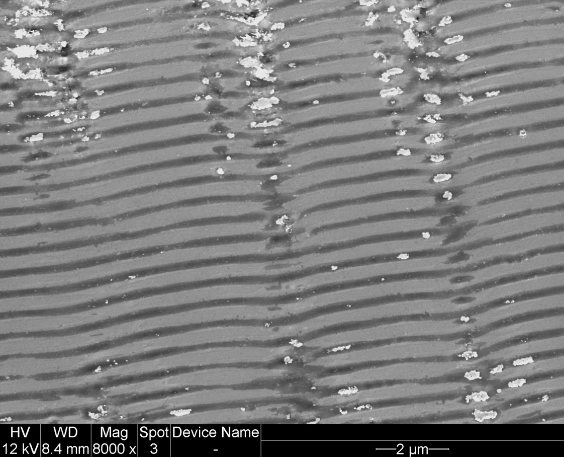
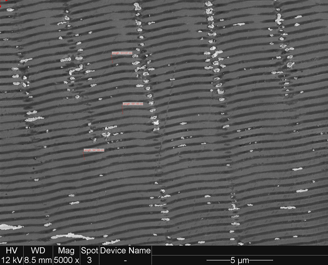
Figure 1b. SEM images of highly uniform LIPSS created at a fluence of 0.8 J/cm2 at 8000x magnification
Figure 1a. SEM images of highly uniform LIPSS created at a fluence of 0.8 J/cm2 at 5000x magnification
SEM images revealed that the LIPSS had a period of 532 nm and a fill factor of 75%. The depth of the channels was found to increase with increasing fluence. At 0.8 J/cm2, highly uniform structures were obtained with no surface material removal. The periodic structures appeared to have a flat top surface with filleted edges and deep, narrow valleys. The depth of the valleys was determined through atomic force microscope imaging and was found to range from 150 nm to 350 nm. Fig. 1 shows SEM images of the highly periodic LIPSS created at a fluence of 0.8 J/cm2. At higher fluence values up to 1 J/cm2, the valley depth was found to increase and light was trapped more effectively. At a fluence of 1.1 J/cm2, deep and continuous LIPSS were formed, resulting in an average reflectance of 23.1% corresponding to a 35.7% decrease in average reflectance compared to bare silicon. At even higher fluence values up to 1.2 J/cm2, deep valleys were created with irregularities due to material removal. This resulted in even lower reflectance values due to increased scattering of light below the surface of the material. Beyond this fluence value, the structures no longer appeared periodic. Deep craters and surface irregularities were formed which further enhanced scattering and light trapping below the surface, thus decreasing the average reflectance. Fig. 2 shows the reflectance curves for structures created at different fluence values, across the wavelength range of 400 nm to 860 nm. A clear decreasing trend in reflectance is seen as the fluence is increased. Above this fluence, material removal causes severe damage to the surface.
Figure 2. Reflectance curves showing a decreasing trend in reflectance with increasing fluence values
In order to measure the broadband reflectance of the sample, a Perklin Elmer spectrophotometer was used. First, the sample was checked for opacity, and then the spectral reflectance (R) and transmittance (T) were measured over the wavelength range of 200 nm to 1200 nm. A monochromator was used to resolve the wavelength. Structures made with increasing fluence values exhibited a trend of decreasing average reflectance value. As the fluence was increased from 0.95 J/cm2 to 1.4 J/cm2, the average reflectance over the wavelength range of 400 nm to 860 nm decreased from 25.79% to 19.84%. Fig. 2 shows the reflectance curves for structures created at different fluence values, across the wavelength range of 400 nm to 860 nm. As compared to the reflectance of bare silicon which was measured to be 35.93% over the same wavelength range, a 44.8% decrease in reflectance was achieved for the case of texturing at 1.4 J/cm2. This drop is attributed to the increasing depth of channels and increasing irregularities on the surface.
In summary, silicon wafers with average reflectance values of 23.1% were fabricated by texturing the surface with a picosecond laser. These structures were created at high laser scanning speeds of 4000 mm/s and low pulse overlapping ratios of 60%. Picosecond lasers, due to their lower power density, high rep. rate, and high pulse energy, were shown to be ideal for high-speed surface texturing. With the availability of high-power, high-repetition picosecond laser, the processing speed can further increase, offering the possibility of surface texturing during roll-to-roll manufacturing processes. This method provides an inexpensive and rapid process to create low-reflectance silicon wafers which can be used in photovoltaic applications.
Yung C. Shin is a professor and director at the Center for Laser-based Manufacturing for the School of Mechanical Engineering at Purdue University.
References:
1.) M. A. Green, K. Emery, Y. Hishikawa, W. Warta and E. D. Dunlop, Solar cell efficiency tables (Version 45), Prog. Photovolt: Res. Appl. 2015, 23:1–9
2.) J. I. Gittleman, E. K. Sichel, H. W. Lehmann, and R. Widmer, Textured silicon: A selective absorber for solar thermal conversion, Appl. Phys. Lett. 35, 742 (1979), http://dx.doi.org/10.1063/1.90953
3.) A.W. Smith and A. Rohatgi, A new texturing geometry for producing high efficiency solar cells with no antireflection coatings, Sol. Energ. Mat. Sol. Cells 29 (1993) 51-65
4.)S. Winderbaum, O. Reinhold, F. Yun, Reactive ion etching (RIE) as a method for texturing polycrystalline silicon solar cells, Sol. Energ. Mat. Sol. Cells 46 (1997) 239-248
5.) D.H. Macdonald, A. Cuevas, M.J. Kerr, C. Samundsett, D. Ruby, S. Winderbaum, A. Leo, Texturing industrial multicrystalline silicon solar cells, Sol. Energ. 76 (2004) 277–283
Leading up to the Laser Institute of America’s 50th Anniversary in 2018, I decided to visit longtime industry partners around the country to get a firsthand look at innovations within the laser
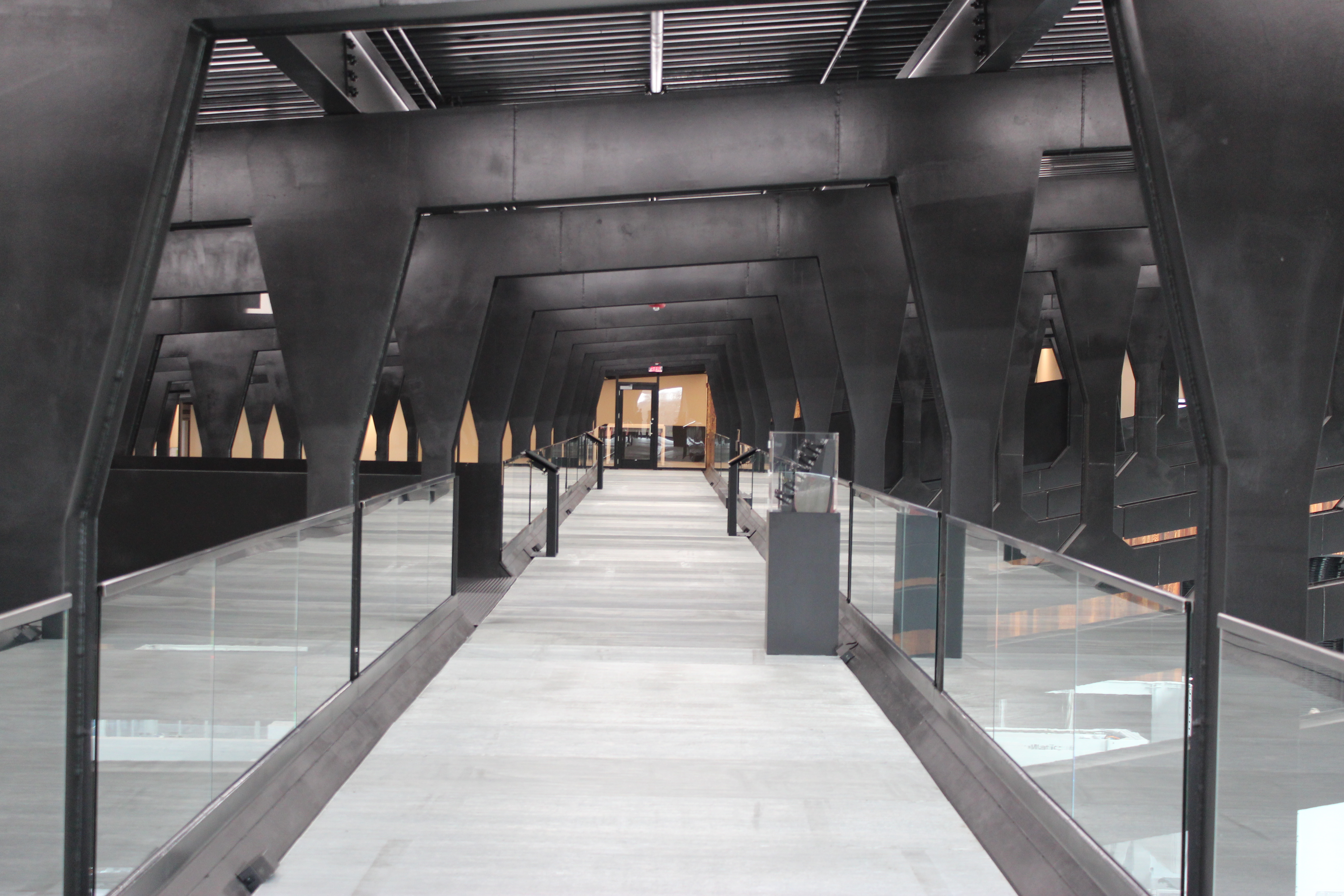
Trumpf Factory (Photo by Jim Naugle)
industry. I was impressed with many of our allies; advancements in the additive manufacturing industry, significant leadership shifts and refreshing concepts seemed to be the common narrative. However, one company took the cake when I visited their 50,000 sq. ft. technology center in Hoffman Estates, Illinois, Nov. 2017. TRUMPF GmbH, a laser systems manufacturer based in Germany, designed and built this $30 million USD manufacturing facility with the future in mind.
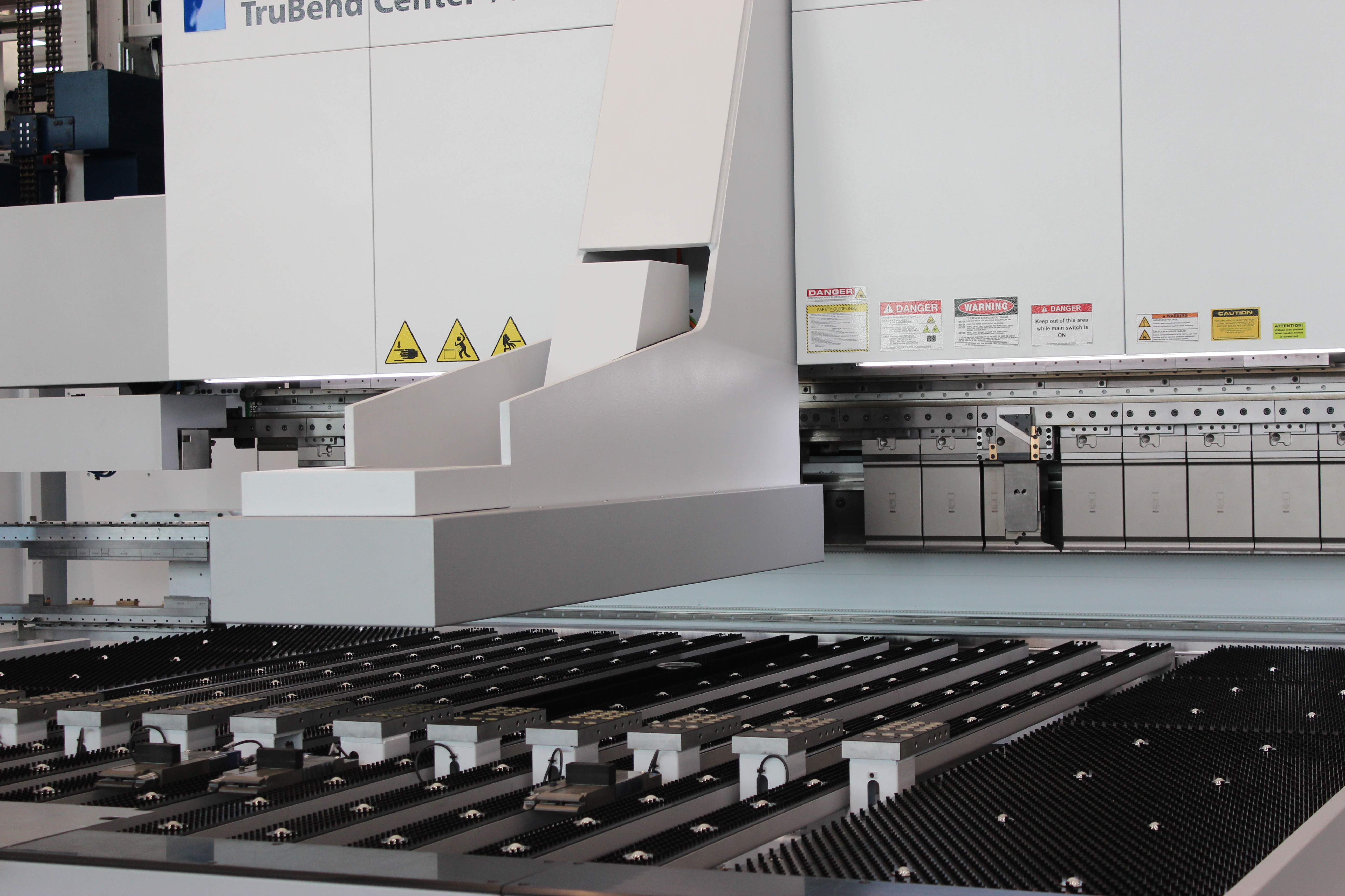
Their state of the art manufacturing and consulting location will educate costumers interested in digitally connected production while showcasing Industry 4.0 Solutions. During my tour of the facility, Jens Kappes, the chief engineer of the Smart Factory, explained that the factory is designed to produce parts using the latest production technologies and strategies.
“TRUMPF Inc. always strives to find new ways to innovate and stay at the forefront of Industry 4.0,” said Kappes. “The TRUMPF Smart Factory is not only a showroom, but also a production site focusing on the entire sheet metal process chain. Every machine is important, but creating an optimized process where everything works together is what we call TruConnect, and critical to an Industry 4.0 facility. The ultimate goal of the Smart Factory is to help our customers introduce digitally connected production solutions into their own facilities. Our Smart Factory intelligently connects the entire sheet metal process chain, and not only improves our own processes but serves as a model for customers to improve their own.”
The organization chose prime real-estate, because according to their website, approximately 40 percent of North America’s sheet metal is processed in the Midwest. This means TRUMPF GmbH
Trumpf Factory (Photo by Jim Naugle)
can better serve customers in the U.S., which is the company’s second largest market after Germany.
The custom built edifice is unique because its architectural design is directly tied to its day-to-day functionally. They didn’t build this beautiful structure to house production, they built it to monitor, adjust and appreciate production in its entirety. It features a self-supporting steel ceiling covering a 55 meter production hall; skywalks that offer a birds eye view; and a futuristic control room that would make Tony Stark proud.
“It was a pleasure to have Jim visit our facility in Illinois and learn about our technology,” said Tobias Reuther, director of TRUMPF’s Smart Factory. “The relationships we foster and maintain with other organizations are important to us. They’re not only critical to our success, but to driving education and growth within our industry.”
I have visited many of TRUMPF’s facilities around the word and each time I leave, I say to myself, “Wow! That’s how you do it!”
From customer service to production ingenuity; Illinois is no different. It truly represents what the future of manufacturing will be and you can see it working to perfection. It’s a must visit for all manufacturing enthusiasts, laser focused or not.