Laser direct writing: An effective approach to flexible hybrid electronics

As featured in the LIA TODAY and ICALEO 2017

By Jinguang Cai and Akira Watanabe

The development of miniaturized portable and wearable electronic devices has attracted worldwide research attention, due to their increasing integration with human daily life. Different from traditional electronic devices on “hard” boards, such devices should be soft and flexible. A concept called “flexible hybrid electronics”, which is a hybrid of soft and hard parts, has been proposed to address the fabrication issue of flexible devices.

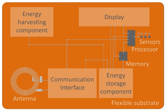
Fig. 1. A schematic image of a simple flexible hybrid electronic device.

The concept of a flexible hybrid electronic device is illustrated in Fig.1, in which “soft parts”, such as electronic interconnection, energy harvesting and energy storage components, antennae, and even displays, sensors, and communication interfaces, can be prepared via printing methods. “hard parts”, such as processor and memory, can be provided by the commercial small-size silicon components, which are small enough, and can be integrated into the device without influencing the flexibility. However, printing methods have some issues such as limitation of materials, high cost of inks, and complicated post-processing.

Laser direct writing is a non-contact, fast single-step fabrication technique without requirements for masks, post-processing, and complex clean environments. Meanwhile, various kinds of lasers have been rapidly developed with relatively low costs and broad available wavelengths and powers, and widely used in industry for materials welding, cutting, and polishing. Besides, laser processing can be focused into a micrometer-sized or submicrometer-sized area to realize on-demand fabrication of functional micro-patterns, showing the potential to be integrated into current product lines for commercial use. Laser direct writing has been demonstrated to prepare energy harvesting and energy storage components, electronic circuits, sensors, communication interface, and antennae.

Energy harvesting and storage components

Generally, a flexible device employs a thin film battery as the energy storage and supply unit, in combination with a flexible energy harvesting device such as a polymer solar cell. Recently, as a new type of energy storage device, micro-supercapacitors (MSCs), has been developed and recognized as potential power supply units for on-chip micro-devices, because they possess not only the advantages of supercapacitors such as high power density, excellent cycling stability, pollution-free operation, maintenance-free feature, and flexibility, but also simplified packaging processes and compatibility with integrated circuits. Among various materials for supercapacitors, carbon materials possess the properties which can satisfy the requirements of MSCs in the flexible devices, such as high specific surface area, high electrical conductivity, high electrochemical stability, and high mechanical tolerance.

Fig. 2. A carbon micro-supercapacitor prepared by laser direct writing.

Laser-induced carbonization of polymers such as polyimide has been demonstrated to prepare flexible all-solid-state carbon-based MSCs with high performance by laser direct writing on a polyimide (PI) film in air (Fig. 2). In order to suppress the oxidation process and thus, increase the conductivity of the laser-induced carbon structures, the laser direct writing was conducted on PI films in an inert gas such as Ar, resulting in carbon MSCs with improved volumetric energy density and power density. Furthermore, high-conductive Au nanoparticles can be incorporated to construct double-layer carbon/Au composite electrodes with improved conductivity by two-step laser direct writing.

It will be beneficial for practical use if energy harvest and storage units can be integrated into the same device. As a demonstration, TiO2 nanoparticles were deposited on one side of the laser-written interdigitated carbon electrodes by an electrophoretic method, forming carbon/TiO2 composite MSC with photo-rechargeable capability under UV irradiation due to the photovoltaic property of TiO2 nanoparticles. Although the charging voltage is not high enough for practical use currently, it is expected that such a strategy can be developed for practical use by optimizing the photo-absorption materials and the combination.


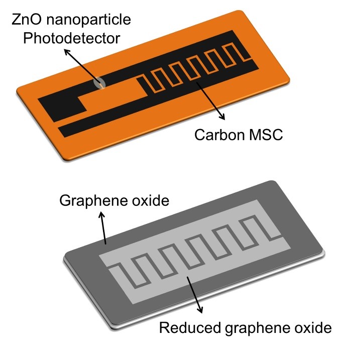
Fig. 3. Schematic images of an integrated photodetector (top) and a rGO/GO/rGO humidity sensor (bottom) prepared by laser direct writing.


Photodetectors and humidity sensors

Sensors are one of the most important interfaces with users in IoT (Internet of Things) technology, thence it is very important to develop various types of sensors for flexible devices. Laser direct writing can play an important role in preparing sensors directly on the flexible substrate with high performance and stability. For example, a photodetector for UV light can be fabricated by laser direct writing and deposition of ZnO nanoparticles, and can be integrated into the PI film with a carbon MSC fabricated by laser-induced carbonization, forming an integrated photodetector for practical use (Fig. 3, Top). Besides, a humidity sensor based on an interdigitated reduced graphene oxide (rGO)/graphene oxide (GO)/rGO structure prepared by laser direct writing was also demonstrated with high and fast response, flexibility, and long-term stability, showing the potential to be used in flexible devices (Fig. 3, Bottom).

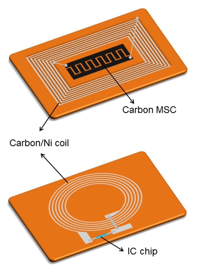
Fig. 4. Schematic images of an integrated wireless charging and storage device (top) and an NFC tag (bottom) prepared by laser direct writing in combination with electroless Ni plating.

Circuits, communication interface, and antenna

High-conductive metallic circuits with mechanical stability are very important in flexible devices as basic structures, and their preparation should be facile, cost-effective, and easily integrated with other electronic components. Laser direct writing has been demonstrated to pattern metallic Pd on PI films, which can act as catalysts in the electroless Ni plating process, producing high-conductive carbon/Ni composite structures. The carbon/Ni structures exhibited a certain flexibility and excellent anti-scratch performance due to the intimate deposition of Ni layer on carbon surfaces. Such carbon/Ni structures can be used as conductive circuits to construct practical devices.  For example, a wireless charging and storage device can be fabricated by integrating an outer rectangle carbon/Ni composite coil for harvesting electromagnetic waves and an inner carbon MSC for energy storage, which can be fast charged by a commercial wireless charger (Fig. 4, Top). In addition, a near-field communication (NFC) antenna was prepared using a carbon/Ni composite coil, and acted as a communication interface with an NFC smartphone for harvesting signals, and an ultra-small commercial IC chip was integrated for data storage (Fig. 4, Bottom). The integrated NFC tag can be used for practical application.

Summary & outlook

While laser direct writing has been demonstrated to be an effective approach to preparing most of the components in flexible devices, such as carbon MSCs as energy storage unit, carbon/TiO2 MSCs for energy harvesting and storage unit, photodetectors and humidity sensors, high-conductive carbon/Ni structures for electronic circuits, and even integrated wireless devices, many efforts are still required to promote the laser direct writing technique applied in the development of flexible hybrid electronics for practical applications in IoT in the future.


Jinguang Cai, Institute of Materials, China Academy of Engineering Physics, Jiangyou 621908, Sichuan, P. R. China

Akira Watanabe, Institute of Multidisciplinary Research for Advanced Materials, Tohoku University, 2-1-1 Katahira, Aoba-ku, Sendai 980-8577, Japan

Inventors Synthesize Graphene with Lasers

As featured in the LIA TODAY

By Liliana Caldero

Graphene – it’s the two-dimensional (2D) allotrope of carbon atoms that ignited the imaginations of researchers across the globe. Heralded as a ‘miracle material’, its potential seemed limitless and it was predicted to usher in the next generation of technology. Flexible, stronger than steel, transparent, lightweight, and an amazing conductor of heat and electricity, it was going to revolutionize everything from household electronics to biomedical nanotechnology.


THE PROBLEM

Yet, nearly eight years after Dr. Andre Geim and Dr. Konstantin Novoselov earned the Nobel Prize in Physics for first isolating graphene and identifying its properties, graphene has encountered barriers to moving out of the lab and into the marketplace. According to Prof. Dr. Aravinda Kar of the University of Central Florida’s Center for Research and Education in Optics and Lasers (CREOL), one of the most prominent barriers has been finding scalable manufacturing processes that can produce graphene of a quality and quantity ready for consumers and businesses.

Graphene is notoriously difficult to synthesize in large quantities at a consistent quality. Early methods of isolating graphene involved a slow and tedious mechanical exfoliation technique; the researchers would extract a thin layer of graphite from a graphite crystal using regular adhesive tape, continually reducing the graphite sample by sticking the tape together and pulling it apart until only a small, 2D section of carbon atoms with a honeycomb lattice remained. Graphene’s unique characteristics are only present when it is one, two, or three layers of atoms thick – any thicker and it becomes graphite, losing all of the exceptional properties of graphene. The tape exfoliation method, although useful for the lab, was not going to translate very well to an industrialized process.


SOLVENT-AIDED EXFOLIATION AND CVD

Two of the more promising and potentially scalable methods of producing graphene are solvent-aided exfoliation and chemical vapor deposition (CVD). In solvent-aided exfoliation, sonication is used to exfoliate graphene crystals which are then further separated in a solvent and later gathered into graphene monolayers.  Scientists at the National University of Singapore have identified a flocculation method that reduces the amount of solvent needed for their exfoliation process, which could yield graphene using far less solvent than was previously needed. Another method experiencing innovation is CVD, which uses thermal chemical reactions to ‘grow’ graphene on substrates of specific materials, typically copper or silicon. Recently, engineers at MIT developed a CVD process for producing graphene filtration membrane sheets at 5 cm per minute. One of the biggest issues with traditional CVD and exfoliation methods is the need to transfer graphene from its fabrication platform to a substrate. Lasers are going to change that.


THE MISSING PIECE – LASERS

Lasers may provide yet another avenue to the elusive mass production of graphene, with an eye toward innovating the semiconductor industry. In 2003, Kar, along with Dr. Islam Salama and Dr. Nathaniel Quick, realized that laser direct writing could be used to fabricate carbon-rich nanoribbons on a silicon carbide (SiC) wafer in a nitrogen rich environment. Although these ribbons were too thick to be considered graphene, Kar believed that with a few changes, this process could be reworked to synthesize graphene in situ on a large scale, very quickly. In 2013, Kar and Quick were issued a patent for a Laser Chemical Vapor Deposition (LCVD) method that could be scaled for mass production.

Their method involved a few simple components: a frequency doubled Nd:YAG (green) laser of 532 nm wavelength, methane (CH4) gas, a silicon substrate, and a vacuum chamber.

The 532 nm wavelength corresponds to a photon of energy 2.33 eV, so the energy of two photons is 4.66 eV, just within the range of the C-H bond energy (4.3-4.85 eV) in CH4. Focusing the laser beam to a high intensity can induce two-photon absorption at the focal plane, causing the decomposition of CH4 to release the hydrogen atoms and deposit carbon atoms only on the substrate. The laser heating of the silicon substrate is just low enough to avoid melting the silicon, while providing sufficient thermal and electromagnetic energies to assist the carbon-carbon bonds rearrange into graphene’s trademark hexagonal pattern.

An experimental set-up for multiphoton photolytic laser chemical vapor deposition (LCVD) of graphene from methane precursor. Image courtesy of Dr. Kar and Dr. Quick.

LASER DIRECT WRITING OF GRAPHENE

Kar believes this process could be adapted to add graphene directly onto any substrate. Using laser direct writing, a company could easily draw graphene circuits onto a board. For companies using a hybrid approach, the graphene could be deposited at precise points as interconnects. “You would have all the CAD/CAM capability you could want,” says Quick. Currently, green lasers are available at high output powers, 100 W in continuous wave mode from most large laser manufacturers, so adding this additional step to the manufacturing pipeline for semiconductors would be easy and inexpensive compared to other methods.

At 1.9 cm per second, or 45 inches per minute, this method of graphene production is fast and efficient. This LCVD method offers control over the number of graphene layers, whether one, two, or three are required.  This process also removes the need to manually place graphene onto its intended location, as it is synthesized precisely where it should be. It’s also worth mentioning that this process is conducive to minimal environmental impact, as the unreacted methane and hydrogen byproducts can be captured to be recycled and reused.


A LOOK AT THE FUTURE

Picture this: a template is placed over a substrate and a line-shaped laser beam sweeps over it briefly or a beam of large cross-sectional area illuminates the entire template in one shot; when the template is removed, an intricate graphene design has been printed onto a circuit board. That is the future that Kar says is possible, with the right equipment. He suggests that we need manufacturers to develop lasers producing line-shaped beams or large area beams with spatially uniform intensity profile to realize this vision cost-effectively. He emphasizes that a true line-shaped beam produced by a slab laser system or an array of optical fiber laser would be necessary, as shaping the beam synthetically by changing the shape of an aperture would result in too much lost energy. With this technology, graphene could easily be printed onto circuit boards immediately, only where it’s needed, saving in material costs and time.

Nearly 14 years after the excitement first began, researchers are still exploring the potential uses of graphene; from applications in microsupercapacitors to Organic LEDs in flexible displays to ultra-sensitive optical sensors, and even lightweight body armor, the possibilities are still as exciting as ever.


Acknowledgements

Prof. Dr. Aravinda Kar, University of Central Florida, CREOL

Dr. Nathaniel Quick, Executive Director of LIA


LEARN MORE

Laser Formation of Graphene: United States Patent 8617669. (N. Quick, A. Kar)
http://www.freepatentsonline.com/8617669.html

NUS-led research team develops cost effective technique for mass production of high-quality graphenehttp://news.nus.edu.sg/press-releases/mass-production-graphene-slurry

MIT researchers develop scalable manufacturing process for graphene sheetshttps://newatlas.com/mit-manufacturing-graphene-filtration-membranes/54274/

Design Guidelines For Laser Metal Deposition of Lightweight Structures

Design Guidelines for Laser Metal Deposition of Lightweight Structures

By Ake Ewald and Josef Schlattmann

Introduction

Weight critical applications, like parts in the aerospace industry, are driven by lightweight design. Titanium alloys have great potential in lightweight design of structural parts due to their excellent specific mechanical properties. Today, structural parts are manufactured in conventional milling processes. Titanium parts are characterized by poor milling behaviour as well as high material waste rates up to 95 % [1]. The Laser Metal Deposition (LMD) is a layer-wise manufacturing process for the production of three-dimensional complex parts [2].

LMD builds parts based on a nozzle-fed powder, which is solidified by a laser. The process can be used for surface cladding, repair and build-up of parts. For an effective industrial application, it is necessary to identify all advantages and disadvantages. A lowering of the introduction barrier can be achieved by design guidelines helping the engineer early in the product development. With LMD like Selective Laser Melting (SLM), existing manufacturing guidelines cannot be simply adopted. Due to the complex process constraints, a design guideline for LMD has been established.

Complex parts often share simple geometries as a basis. These shapes were identified and used to evaluate the applicability and effectiveness of LMD. Following established lightweight design guidelines, the presented guideline focuses on fine structures. In addition to the manufacturability, the building accuracy and the surface roughness have been investigated, since both have a significant influence on the product quality and the necessity of post processing towards the final shape of a part.

Investigation of process constraints

The investigations are performed with a Trumpf TruDisk 6001 multi-mode continuous wave disk laser with a laser power of 6 kW at a wavelength of 1.03 µm. A three nozzle processing head is used with a rotational table feeder (Fig. 1). The used Ti-6Al-4V powder is spherical and sieved to a fraction less than 80 µm.

Figure 1 Robot cell (TruLaserRobot).

Three different building strategies have been identified in a preliminary design guideline by Möller et al., 2016 [3]. Figure 2 shows the different building strategies. In S1 an inclination is achieved by a stepwise offset (a) between the layers (α = β = 0°). S2 rotates the platform to reach the inclination. The structure is manufactured vertically without an offset between the layers. S3 rotates the machine head to the inclination angle of the structure. The structure can be manufactured without an offset. Besides the three single building strategies, combinations of these are possible, which are not considered at this point. The preliminary guideline published by Möller et al. (2016) showed a high potential in the degree of freedom of building strategy S2 and S3 [3]. For this reason, these strategies were further investigated.

Figure 2 S1: horizontal offset between layer, S2: rotation of platform, S3: rotation of machine head

The mentioned fine structures have been classified as thin walls, curved walls, congregating and aggregating structures. The width of the manufactured structures has been set to a single layer width. The length has been set to 50 mm.

Thin Walls

The build-up of inclined thin walls has been made to investigate

  • the connection towards the platform,
  • the influence of the gravitation,
  • the building accuracy and
  • the influence on the wall surface.

Both strategies produce a constant and comparable wall thickness under (see Fig.3). It varies due to the surface roughness of about 150 µm. The variation of the measured angle is less than 1°.

Figure 3 Measured wall thickness of the inclined walls manufactured with S2 and S3.

The surface quality of a part has an influence on the appearance, the buy to fly ratio in case of a post processing, and the fatigue strength. The mean values of the surface roughness remain constant with rising inclination angles. The surface roughness of S3 is about 15 µm higher than with S2.


Curved Walls

Curved walls can vary in radius and angle. Curved walls can be divided into curves with their rotational axis parallel, and perpendicular to the building direction (z-axis, Fig. 4). The vertical built up of the curved walls with different radii can be seen in fig. 5.

Figure 4 Sketch of curved elements perpendicular (a) to the building direction and (b) parallel to the building direction.


Figure 5 Set of manufactured parallel curved elements with radius of 0 mm (left) to 30 mm (right).

The radii of the built walls are 0.15 mm to 0.4 mm smaller than expected. An intended vertical edge (radius of 0 mm) produces an outer radius of 3.58 mm. Without post processing, edges should be designed to allow a radius up to the layer width. The radius independent deviation allows the manufacturing in reproducible tolerance fields.

Congregating and Dividing Structures

The separation in congregating and dividing structures is based on the necessity of different manufacturing strategies and constraints in LMD (Fig. 6).

Figure 6 Sketch of the three defined congregating and dividing structures with building direction in z: (a) Y-branch, (b) overhang and (c) reversed Y-branch.

The manufacturing of regular and reversed Y-branches was realised by using S3. To achieve good results, binding on alternating branch sides is recommended (Fig. 7).


Figure 7 Sketch of the Y-branch (above), manufactured Y-branches with the angles β1 = β2 = 30° and β1 = β2 = 45° (below).


Additionally, overhangs were built on the manufactured vertical wall (Fig. 8) to evaluate

  • the connection between a thin rough wall and a manufactured wall,
  • the building accuracy, and
  • the boundary constraints.

The measured angles of the overhangs have an angle deviation of less than 1° up to a manufacturing angle square to the gravity (Tab. 1). This is comparable to the inclined walls. Overhangs show that overhangs with the same or smaller width can be manufactured on thin walls.

Figure 8 Manufactured overhangs with inclination angles from 30° to 90°.


Table 1 Measured inclination angles of the manufactured overhangs. The guidelines derived from the experimental investigation have been collected in a design catalogue according to the VDI 2222 in extracts shown in the figure 9.


Figure 9 Detail from the established design catalogue

Conclusion and Outlook

LMD offers a high degree of freedom in the design of parts. Lightweight parts can benefit from this flexibility. An industrial application can be achieved by design guidelines helping engineers to take the advantages and disadvantages of the LMD process into account during the design process.

The experimental investigation points out that structures based on the basic shapes are producible with constant geometric and surface tolerances, which allows reliable final machining. This is the basis for a successful design process. The building strategy S2 and S3 can be applied. The comparable results of S2 and S3 allow to choose the better fitting strategy for a specific use case.

By focusing on lightweight application, the following aspects have been achieved:

  • Investigation and manufacturing of basic shapes
  • Determination of process constraints
  • Draft of a design guideline.

The developed design catalogue builds a first step towards a comprehensive design guideline for LMD.


M.Sc. Ake Ewald has been a research assistant in the workgroup System Technologies and Engineering Design Methodology at the Hamburg University of Technology since 2013. He works in the methodical product development where he researches the methodical design of hybrid manufactured structural parts using LMD.

Josef Schlattmann is Univ.-Professor at the Hamburg University of Technology. He leads the workgroup System Technologies and Engineering Design Methodology.


References

[1] Allen, J. (2006) An Investigation into the Comparative Costs of Additive Manufacture vs. Machine from Solid for Aero Engine Parts, Rolls-Royce PLC Derby, UK.

[2] Ravi, G.A., Hao, X.J., Wain, N., Wu, X., Attallah, M.M. (2013) Direct laser fabrication of three dimensional components using SC420 stainless steel, Materials & Design, Vol. 47, 731-736.

[3] Möller, M., Baramsky, N., Ewald, A., Emmelmann, C., Schlattmann, J., (2016) Evolutionary-based Design and Control of Geometry Aims for AMD-manufacturing of Ti-6Al-4V Parts, Laser Assisted Net Shape Engineering 9 International Conference on Photonic Technologies Proceedings of the LANE 2016, S. 733–742, DOI: 10.1016/j.phpro.2016.08.075.

Diode Lasers in Cladding, Additive and Hybrid Manufacturing

By Oleg Raykis

Today there exist a number of technologies for additive manufacturing of components.

The two most prominent types utilizing lasers for generating parts out of metals are either powder bed based solutions or direct energy deposition, often referred to as laser metal deposition. As a company Laserline focuses mainly on the second type. Depending on the application it allows you to produce larger part sizes with higher productivity (deposition rates and therefore higher productivity) due to the fact of not being limited by the size of the building chamber as it would be in the case of a powder bed machine. It is also much faster in many cases.

Laserline identified four main application areas for AM in which we operate and be described based on examples in this article. Those areas include, besides generating complete parts by terms of additive manufacturing, also repair welding application or hybrid machines – a combination of conventional machining and laser technology the fourth main application area would be providing functional areas on conventionally manufactured parts.

Additive manufacturing technology allows generating shapes and structures in a single production step with little material loss, post machining and tool wear (near-net-shape manufacturing). Thereby you can use material in powder or wire form. The advantage of using wire is that you will have a 100% material utilization; the compromise on the other hand might be the directional dependency when you supply the wire laterally and not coaxial. Pic. 1 shows an example of a free form application as a rocket nozzle demonstrator part made out of Inconel 625.

Pic.1 Free form powder AM of a rocket nozzle demonstrator (Source: Fraunhofer CLA)

The part was done without any type of process control. Another interesting example of AM with Titanium is shown in Pic.2.

Pic. 2 Ti64 powder AM with closed loop process control (Source: Fraunhofer CLA)

Compared to the rocket nozzle, process control was used when producing the demonstrator part in pic.2. The camera based system (in this case E-MAqS) is capable of measuring the size and temperature of the melt pool. Furthermore it can give feedback to the laser source and adjust the laser power accordingly to maintain the desired size of the melt pool. This in turn ensures consistent reproducible part build ups with no defects.

Another very interesting and promising approach is to integrate the laser source into machine tools. There are several hybrid machine tool concepts being developed; one of them is the combination of additive and subtractive tools which achieves a new level of manufacturing. One example is the merger of a laser with a 5-axis milling machine. The integrated diode laser deposits the powdered metal layer by layer, generating a solid, fully dense metal part. The following milling operations directly finish machines surfaces in areas necessary, without changing setup.

Pic.3 An example of a conventional milling machine with integrated AM technology (Source: DMG Mori-Seiki)

This flexible switch between laser and mill also allows the machining finish of areas, which would be impossible to reach on the final component. Designs with undercuts, internal geometries and overhangs without support structure are no problem. The manufacturing of completely new structures and designs are now possible. All weldable metals, which are available in powder form, can be used, for example steel, nickel and cobalt alloys as well as titanium, bronze or brass.

A third important field of AM from our perspective are repair welding applications. Probably the most prominent and widely industrially utilized are the repairs of turbine blades. Turbine blades in steam engines, especially in the first two rows, experience a lot of wear through erosion. Instead of replacing the whole part it is possible to repair the worn area by putting a couple of layers (mostly nickel / cobalt based super alloys) and machine them down to the finished surface, see Pic.4.

Pic.4 Turbine blade repair (Source: Fraunhofer ILT)

This remanufacturing procedure saves up to 90% of material and energy cost compared to manufacturing a new blade. Even though turbine blades are the most prominent example of laser repair welding a wide variety of other parts can be restored using the procedure, e.g. worm shafts, helical gears, molds, etc. to name a few. When speaking about additive manufacturing most people have the production of complete parts in mind. This doesn’t always have to be the case. Often it makes more sense from an economic standpoint to add to a conventionally (and relatively inexpensively) produced part functional areas where they are needed. Pic. 5 shows one such example.

Pic. 5 Extruder barrel demonstrator (Source: Fraunhofer CLA)

In this case 100 lbs. of hard and wear resistant Stellite 21 powder material was deposited on a metal pipe base structure to form the extruder thread. One further example of it can be functional layers on drill bits where sensors need to be shielded from magnetic interference. By creating heat resistant layers out of non-magnetic materials it is possible to place those sensors.Through a clever combination of the usage of conventional and additive manufacturing technologies it is possible to produce advanced parts without increasing the cost.

Quality Assurance of Selective Laser Melting Applications

By Thomas Gruenberger

Key differentiation criteria for Additive Manufacturing (AM) technologies are freedom of design, cost advantage, customization, and time to market.

Direct metal laser sintering (DMLS) AM technology is ideal for serial production for industries like aerospace.

Setting up a process means mapping the input parameters (e.g. machine and process parameters and part geometry) to output parameters (part properties like density, tightness, surface quality). An in-situ nondestructive measurement of part properties like density is not possible, so indirect measurements have to be performed. Information from the process – process emissions, melt pool size, melt pool dynamics, and temperature distribution – can be used for this indirect measurement enabling the user to find a correlation between features of these measurements and the resulting part properties. Additionally, a shorter process development time can be achieved by avoiding destructive tests during development learning reading the extracted features (see Fig. 1).

Fig. 1: Quality inspection – the challenge

As mentioned above, several pieces of information from the process can be used for the detection of irregularities, so different sensor technologies can be used. Consider a manual in-situ inspection of the process, where the user looks at the visible process emissions in the process chamber. Differences in brightness, size, color, and number of sparkles can be detected with the human eye. This can be automated using photodiode based meltpool monitoring systems like the plasmo fast process observer, a hardware developed by plasmo with up to 4 channels at sampling rates up to 300kHz.

So the system measures the brightness of the process emissions over time (blue curve in Fig. 2), using CAD data, the data can be mapped easily to an image of brightness of process emissions over the building platform (see Fig. 2 right plot), layer for layer, in pseudo color representation.

Fig. 2: Feature map of the building process

Running an OK process gives the baseline of the feature, provoking process irregularities yields in a change of the feature, enabling the user to set limits for the feature according to its quality needs. A pseudo color representation of a map of process irregularities can be calculated, giving the user an easy way to understand visualization and therefore, fast feedback about the quality of the process. As a note, black means no process irregularities and yellow means 100 percent of process irregularities in the given pixel in Fig. 3.

Fig. 3: Map of process irregularities

The fully automated measurement system enables a 100 percent inspection of the building process. The high sampling rate (ca. 10,000 times fa

ster compared to the human eye) enables the system not only to calculate features like signal height but the additional analysis in time, frequency and time scale domain can be performed, too. Three (3) different algorithms (features) are calculated by the system and each algorithm can be parametrized according to the quality needs for every exposure type used in the layer.

These algorithms are easy to explain. Based on physics, they correspond directly to process different phenomena.

  • Absolute limits: Influences in the size and form of the cross section of one exposure like focal position, laser power and welding speed
  • Signal dynamics: Noisy processes or less process dynamics like pollution, protective gas flow and lack of fusion
  • Short time fluctuations: Short changes in the signal caused by e.g. ejects and pollution

In cooperation with EOS, the described system was integrated with their machines. A typical layout is shown in Fig. 4.

Fig. 4: System layout – EOSTATE Meltpool

As shown in Fig. 4, two total photodiodes are used an onAxis diode measuring the process emissions at the interaction zone of the laser beam and powder and an offAxis diode giving an overview of process emissions about the complete building platform.

A heuristic model is used for setting up the system; therefore, input parameters like process parameters (laser power, scanning speed, gas flow, …) and malfunctions like loss of laser power, and material quality are varied for different building jobs. The output parameters are part properties (porosity, surface roughness, …), process emissions (brightness, temporal behavior, spectral properties, …) and undesired effects like overheating, warpage and lack of fusion. Based on this data set the system can be parametrized to fulfill the quality needs of the customer.

Fig. 5 shows a provoked malfunction, missing powder choosing a too low dosing factor of powder, the irregularities (here red in Fig. 5) can be easily detected.

Fig. 5: Example missing powder, left image of powder bed, right calculated irregularities after exposure

Fig. 6 shows a phenomena process flipping provoked by changing the focal position, the irregularities (red in Fig. 6) can be detected successfully for the complete parts and also the embedded parts (letter F).

Fig. 6: Example process flipping, left image of building platform after complete build, right calculated irregularities

Successful detection of additional phenomena has been shown:

  • Overhanging parts
  • Dust/particles
  • Part overlap
  • Balling / humping
  • SLI pores (simulated porosity)
  • To be continued.

The presented diode based meltpool monitoring system enables the fully automated detection of process phenomena (see Fig. 7) which directly corresponds to part properties.

Fig. 7: Example stable and unstable process, top image of process emissions, middle measured brightness, bottom windowed FFT analysis

Easily understandable algorithms based on physics are applied and can be parametrized by the user according to its needs. A heuristic model for setting up limits was presented and examples of detectable process phenomena are given. The system is part of an integrated quality inspection portfolio at EOS including EOSTATE powderbed and EOSTATE system monitoring.

Further investigations in detectable process phenomena and self-healing effects of defects will be completed. Additional work is in progress in the field of statistical data processing, so information (see Fig. 8, e.g. trends, …) is extracted from data visualized in dashboards enabling the user to perform statistical process control (SPC) at one machine up to different machines at different locations worldwide.

Fig. 8: Statistical process control

About plasmo 

Headquartered in Vienna, Austria, plasmo is an innovative, globally operating technology company for automated quality assurance systems in manufacturing industries. Established in 2003, plasmo leads the way in the real-time quality control of joining processes. The extensive portfolio in the field of quality assurance includes laser power measurement, the monitoring of welding processes, geometric shapes and surfaces, tailor-made solutions in the field of industrial image processing, analysis software as well as an extensive range of services.

With over 700 plasmo systems in operation worldwide, the growing list of clients includes ABB, Benteler, BorgWarner, Faurecia, INA, SMS Siemag, Hettich, JCI, Magna and Valeo to Webasto, and numerous automobile manufacturers such as Audi, BMW, Daimler, Ford, GM, PSA, Suzuki, Volvo as well as various international steel manufacturers. www.plasmo-us.com

© 2017 Dr. Thomas Grünberger, plasmo Industrietechnik GmbH, Vienna