Laser Additive Manufacturing’s Journey to Commercialization

By Andrew Albritton

As seen in LIA TODAY

LASER ADDITIVE MANUFACTURING CHALLENGES

Laser Additive Manufacturing (LAM), as it pertains to powder based manufacturing, is a technique that utilizes the interaction of lasers and base materials to construct a product, rather than removing material from a pre-constructed block of material. LAM is quickly approaching the critical point of being more than a method to produce prototypes and small runs of one-off parts – it is poised to turn everything we know about mass production on its head. Professor Dr. Minlin Zhong, President-Elect of LIA and Director of the Laser Materials Processing Research Center at Tsinghua University, believes it surpasses all available alternative methods.  Prof. Dr. Zhong  says “LAM shows obvious advantages on freeform manufacturing, including free geometry, free structures, free strengthening mechanism, free microstructures, free performance and even free scale (from macro, to meso, to micro, to nano),”. Manufacturers who use LAM are able to reduce the waste of materials commonly associated with traditional subtractive manufacturing methods; decrease the weight of parts by cutting out filler materials; and have more control over material properties resulting in stronger, more complex, lighter, and more efficient parts. With such exceptional technology currently at our disposal, why hasn’t LAM been more widely adopted?

IT’S EXPENSIVE

One of the most commonly cited reasons is that the costs to produce parts through LAM are prohibitive. The key driver of these high costs is that the supply chain for metal powders is not yet optimized for LAM technology. Materials are expensive, custom made, or not readily available. The Metal Powder Industries Federation (MPIF) states in its 2017 PM Industry Roadmap that, “A better understanding of the precursor materials impact on the metal AM process is required. Traditionally, precursor materials have been existing thermal spray powders that have not been refined/tuned to the AM process limiting optimization.” LAM parts producers are often using metal powders that have not been designed for use in LAM processes, which frequently results in suboptimal products.

According to MPIF, as of 2017, there are approximately 12 suppliers of metals for Additive Manufacturing (AM) for the international market, most produce stainless steel, cobalt-chrome, and titanium, with a few supplying aluminum alloys, copper, super alloys, platinum, Inconel, tungsten, molybdenum, and tool steels. With so few suppliers and a sparse number of common material types, there is a bottleneck for providing quality affordable metal powders to the LAM industry. With companies expanding the selection of materials that can be laser processed, it is vital that the problem of material availability be resolved. For example, Nuburu has produced a “blue” laser which operates at the 450 nm wavelength, and is capable of processing gold, aluminum, brass, and copper.

SUPPLY AND DEMAND

What can be done to improve the supply chain and reduce the cost of LAM part production? The metal powder industry does not supply enough quality powder to support widespread adoption of LAM, while early adopters of LAM applications do not create enough demand to drive competition into the metal powder market to reduce prices. A first step to get these industries operating in unison will be the creation and mass adoption of standards, specifications, and best practices in regards to metal powders. By standardizing metal powder properties for best final product properties, metal powder suppliers would be able to build up an inventory without relying on custom special orders. Specifications on how surplus powder from a project can be reused could also help introduce addition cost savings to manufacturers.

STANDARDS FOR QUALITY CONTROL

Another hurdle for LAM is microstructural quality, uniformity, and repeatability. To become a replacement for more legacy manufacturing methods, LAM needs to produce parts consistently and continuously that are to specifications. With traditional subtractive manufacturing methods, there are several quality control points where product is inspected and defects are addressed prior to the next step, resulting in no wasted effort past the point of failure. With LAM, the part in question is created from the ground up; this determines the final product’s quality, microstructure, and mechanical properties simultaneously. The process is completed with either a perfect or defective final product. Paul Denney, Director of Advanced Process Development with IPG Photonics, states, “Unlike machining where you start with a “block” of material with known quality and properties, additive production of parts requires a combination of motion with the prediction of the microstructures, mechanical properties, and stresses. Because the properties are closely connected to how the material is deposited, this greatly complicates the development of processing procedures and parameters.”

What methods can be implemented into a given LAM process to help ensure quality of the final product? The first quality control concerns are addressed long before the process begins. Starting materials must be certified as appropriate for the application, the order of operations of the production device should be scrutinized to ensure that the final product will be to spec with minimal waste, and the machine itself must be operating at peak parameters. As the production of a LAM product can take an extended amount of time, any loss of power to the point of interaction can have detrimental effects to the end product and even the products in queue. Loss of power can be caused by an actual power failure, a dirty or damaged optic, or other origins. With the structural integrity of a LAM part resting critically on the success of every step of the process, it is imperative that the process is stringently optimized and the machine is operating at peak performance. Here is what Paul Denney has to say about the subject:

“Because of the additive manufacturing approach in bed based systems, even if defects can be detected and possibly ‘corrected’, any changes may not be possible. An example of this may be what is done if a ‘defect’ is flagged in a single part in a batch of parts being produced. One approach would be to stop the processing and ‘correct’ the defect. However, if this is done then the thermal history for all of the parts may be altered and all parts may now be out of the desired properties. Another approach would be to stop processing on the part with the defect, but this again would alter the heat load on the complete batch or the time between other parts being produced which may again alter the properties. So any monitoring system will need to detect changes prior to the formation of any defects while at the same time any corrections must be made within the acceptable parameter range.”

There is a thin line between success and failure: one small interruption can ruin an entire batch of product. What can be done to prevent this?

As Paul explained, this is not a single issue, LAM processes need both a method to detect defects and the ability to immediately respond to them. A starting point is to ensure that redundancies are incorporated into the build process so that if a common defect occurs at a certain stage, there are defined responses the system can take automatically to correct them. In the case of a laser lens issue, it may be beneficial to incorporate additional laser delivery systems to the process as a redundancy to pick up where a suboptimal device has failed in real time.

EVALUATING THE FINAL PRODUCT

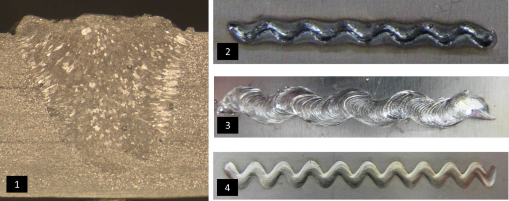
In addition to inline defect detection, the industry as a whole will require a standardized best practice for evaluating finalized parts. For traditional manufacturing methods, a sample of the produced part pool is selected for evaluation via destructive and non-destructive tests to certify whether a set of parts are built to specifications. As many LAM-produced parts are complex and costly to produce, it seems wasteful to destroy a set of them to certify them. In the paper “Evaluation of 3d-Printed Parts by Means of High-Performance Computer Tomography” presented at ICALEO 2017, authors Lopez, Felgueiras, Grunert, Brückner, Riede, Seidel, Marquardt, Leyens, and Beyer reviewed the viability of X-ray Computer Tomography (CT) and 3d scanning as methods to detect inferior AM parts. The paper concludes that the CT method best fits the needs of the AM industry. According to Lopez et. al, “Computer tomography can quantify all complex structures in scope of the proposed demonstrator and delivered deviation values of the measured structure, providing a good base for comparison across demonstrators made by different methods, materials and dimensions. Porosity or defects down to 3 µm can be determined by the used CT system.” Currently, CT scanning a LAM part is a time consuming process, but with additional focus on improvement it could become an essential quality non-destructive control method for finalized parts to evaluate complex internal structures.

TOO MANY ALTERNATIVES

A third barrier to the spread of LAM is the multitude of alternative methods in the industry. As stated by Prof. Dr. Zhong, “Some conventional metal deposition technologies such as arc building-up welding, plasma building-up welding and electronic building-up welding can also fabricate metallic components in near shape. Their deposition rate and productivity may be high and the costs may be lower, but normally they are limited in fabricating complex geometry and accuracy.” Freeform manufacturing is where LAM excels, but despite its many advantages over alternative methods, it has an Achilles heel.

One advantage of alternative manufacturing methods is the speed at which a product can be produced. However, according to Paul Denney, this speed gap is closing faster every day.

“While higher laser powers allow for higher deposition rates but at the expense of lower resolution, some researchers are looking to maintain the resolution by combining multiple lasers into an additive deposition system. Research groups and equipment builders are investigating how best to handle multiple lasers in the same processing area. There are other areas that may be investigated including power distribution to improve the interaction between the power and laser beam to improve efficiency of the process and to minimize defects. This could improve the deposition rates while at the same time maintaining quality.”

Prof. Dr. Zhong hopes that soon LAM researchers will, “improve the materials diversity, increase the dimension (to square meters), increase the deposition rate and decrease costs. A hybrid approach to combine LAM with the conventional additive manufacturing methods may be a solution to achieve the above targets.” The concept of a hybrid production system that can combine multiple lasers with fast alternative methods where complexity is not a requirement could lend itself to faster build times.

THE LATE ADOPTERS

Earlier in the article, we touched on the final barrier to the wide spread success of LAM: industry standards. Current standard offerings from ASTM and ISO cover Design, Materials and Processes, Terminology, and Test Methods. Additionally, new processes are created frequently and new standards are being developed every year in an attempt to keep up. It is unclear how much of the industry has adopted these existing specifications. Until the entire market accepts a set of standards for all steps of the Additive Manufacturing process and supply chain, the evaluation of AM parts will remain a costly endeavor that will limit AM’s potential. MPIF expresses a bleak outlook on metal AM in its State of the PM Industry in North America – 2017 document: “Despite all the fanfare, true commercial long-run production still revolves around only three product classes: titanium medical implants, cobalt-chrome dental copings, and cobalt-chrome aircraft nozzles.” The truth of the matter remains that without a set of clearly defined standards, the LAM industry will continue to remain confined to early adopters like the Aerospace and Medical fields. With the benefits in intricacy and weight saving advantages LAM should have obvious opportunities in the automotive and electronics industries.

Markets are watching LAM for innovative uses before taking the plunge and embracing the technology. Currently, LAM may appear to have a bad Return on Investment (ROI) if producers only hope to replicate their existing products through LAM rather than innovating their parts to capitalize on its strengths. In the words of Paul Denney, “If AM is supposed to make big impact, companies are going to have to rethink their parts; determine how AM allows for changes in the design and possibly improve the performance. The benefits can come in many forms which could be a weight savings, a production savings, and/or a performance savings.” The industry needs to challenge its way of thinking about production to allow the benefits inherent to LAM to propel their production and parts to new levels of performance. Paul Denney provided the following illustration: “With the formation of properties ‘locally’ instead of in ‘bulk,’ it is possible to produce ‘gradient’ materials. The ‘gradient’ can come by changes to the properties of a given chemistry of material or by using materials with different chemistries. As an example: a bracket could be produced for a jet engine that has high temperature properties near the engine but as the bracket extends to an attachment point, the properties/chemistry can be altered to improve the fatigue properties.”

LAM has a bright future and many engineers and scientists are working to unlock its full potential. Once the barriers of the supply chain, dynamic quality control, speed of production, and process standardization have been resolved, it is highly likely the LAM will be a manufacturing method of choice.


ACKNOWLEDGEMENTS

Paul Denney, Director of Advanced Process Development with IPG Photonics and LIA’s Past President

Prof. Dr. Minlin Zhong, Director of Laser Materials Processing Research Center at Tsinghua University

and LIA’s President-Elect


References:

Lopez, E., Felgueiras, T., Grunert, C., Brückner, F., Riede, M., Seidel, A., Marquardt, A., Leyens, C., Beyer, E. (2018). Evaluation of 3D-printed parts by means of high-performance computer tomography. Journal of Laser Applications 30, 032307; https://doi.org/10.2351/1.5040644

Inventors Synthesize Graphene with Lasers

As featured in the LIA TODAY

By Liliana Caldero

Graphene – it’s the two-dimensional (2D) allotrope of carbon atoms that ignited the imaginations of researchers across the globe. Heralded as a ‘miracle material’, its potential seemed limitless and it was predicted to usher in the next generation of technology. Flexible, stronger than steel, transparent, lightweight, and an amazing conductor of heat and electricity, it was going to revolutionize everything from household electronics to biomedical nanotechnology.


THE PROBLEM

Yet, nearly eight years after Dr. Andre Geim and Dr. Konstantin Novoselov earned the Nobel Prize in Physics for first isolating graphene and identifying its properties, graphene has encountered barriers to moving out of the lab and into the marketplace. According to Prof. Dr. Aravinda Kar of the University of Central Florida’s Center for Research and Education in Optics and Lasers (CREOL), one of the most prominent barriers has been finding scalable manufacturing processes that can produce graphene of a quality and quantity ready for consumers and businesses.

Graphene is notoriously difficult to synthesize in large quantities at a consistent quality. Early methods of isolating graphene involved a slow and tedious mechanical exfoliation technique; the researchers would extract a thin layer of graphite from a graphite crystal using regular adhesive tape, continually reducing the graphite sample by sticking the tape together and pulling it apart until only a small, 2D section of carbon atoms with a honeycomb lattice remained. Graphene’s unique characteristics are only present when it is one, two, or three layers of atoms thick – any thicker and it becomes graphite, losing all of the exceptional properties of graphene. The tape exfoliation method, although useful for the lab, was not going to translate very well to an industrialized process.


SOLVENT-AIDED EXFOLIATION AND CVD

Two of the more promising and potentially scalable methods of producing graphene are solvent-aided exfoliation and chemical vapor deposition (CVD). In solvent-aided exfoliation, sonication is used to exfoliate graphene crystals which are then further separated in a solvent and later gathered into graphene monolayers.  Scientists at the National University of Singapore have identified a flocculation method that reduces the amount of solvent needed for their exfoliation process, which could yield graphene using far less solvent than was previously needed. Another method experiencing innovation is CVD, which uses thermal chemical reactions to ‘grow’ graphene on substrates of specific materials, typically copper or silicon. Recently, engineers at MIT developed a CVD process for producing graphene filtration membrane sheets at 5 cm per minute. One of the biggest issues with traditional CVD and exfoliation methods is the need to transfer graphene from its fabrication platform to a substrate. Lasers are going to change that.


THE MISSING PIECE – LASERS

Lasers may provide yet another avenue to the elusive mass production of graphene, with an eye toward innovating the semiconductor industry. In 2003, Kar, along with Dr. Islam Salama and Dr. Nathaniel Quick, realized that laser direct writing could be used to fabricate carbon-rich nanoribbons on a silicon carbide (SiC) wafer in a nitrogen rich environment. Although these ribbons were too thick to be considered graphene, Kar believed that with a few changes, this process could be reworked to synthesize graphene in situ on a large scale, very quickly. In 2013, Kar and Quick were issued a patent for a Laser Chemical Vapor Deposition (LCVD) method that could be scaled for mass production.

Their method involved a few simple components: a frequency doubled Nd:YAG (green) laser of 532 nm wavelength, methane (CH4) gas, a silicon substrate, and a vacuum chamber.

The 532 nm wavelength corresponds to a photon of energy 2.33 eV, so the energy of two photons is 4.66 eV, just within the range of the C-H bond energy (4.3-4.85 eV) in CH4. Focusing the laser beam to a high intensity can induce two-photon absorption at the focal plane, causing the decomposition of CH4 to release the hydrogen atoms and deposit carbon atoms only on the substrate. The laser heating of the silicon substrate is just low enough to avoid melting the silicon, while providing sufficient thermal and electromagnetic energies to assist the carbon-carbon bonds rearrange into graphene’s trademark hexagonal pattern.

An experimental set-up for multiphoton photolytic laser chemical vapor deposition (LCVD) of graphene from methane precursor. Image courtesy of Dr. Kar and Dr. Quick.

LASER DIRECT WRITING OF GRAPHENE

Kar believes this process could be adapted to add graphene directly onto any substrate. Using laser direct writing, a company could easily draw graphene circuits onto a board. For companies using a hybrid approach, the graphene could be deposited at precise points as interconnects. “You would have all the CAD/CAM capability you could want,” says Quick. Currently, green lasers are available at high output powers, 100 W in continuous wave mode from most large laser manufacturers, so adding this additional step to the manufacturing pipeline for semiconductors would be easy and inexpensive compared to other methods.

At 1.9 cm per second, or 45 inches per minute, this method of graphene production is fast and efficient. This LCVD method offers control over the number of graphene layers, whether one, two, or three are required.  This process also removes the need to manually place graphene onto its intended location, as it is synthesized precisely where it should be. It’s also worth mentioning that this process is conducive to minimal environmental impact, as the unreacted methane and hydrogen byproducts can be captured to be recycled and reused.


A LOOK AT THE FUTURE

Picture this: a template is placed over a substrate and a line-shaped laser beam sweeps over it briefly or a beam of large cross-sectional area illuminates the entire template in one shot; when the template is removed, an intricate graphene design has been printed onto a circuit board. That is the future that Kar says is possible, with the right equipment. He suggests that we need manufacturers to develop lasers producing line-shaped beams or large area beams with spatially uniform intensity profile to realize this vision cost-effectively. He emphasizes that a true line-shaped beam produced by a slab laser system or an array of optical fiber laser would be necessary, as shaping the beam synthetically by changing the shape of an aperture would result in too much lost energy. With this technology, graphene could easily be printed onto circuit boards immediately, only where it’s needed, saving in material costs and time.

Nearly 14 years after the excitement first began, researchers are still exploring the potential uses of graphene; from applications in microsupercapacitors to Organic LEDs in flexible displays to ultra-sensitive optical sensors, and even lightweight body armor, the possibilities are still as exciting as ever.


Acknowledgements

Prof. Dr. Aravinda Kar, University of Central Florida, CREOL

Dr. Nathaniel Quick, Executive Director of LIA


LEARN MORE

Laser Formation of Graphene: United States Patent 8617669. (N. Quick, A. Kar)
http://www.freepatentsonline.com/8617669.html

NUS-led research team develops cost effective technique for mass production of high-quality graphenehttp://news.nus.edu.sg/press-releases/mass-production-graphene-slurry

MIT researchers develop scalable manufacturing process for graphene sheetshttps://newatlas.com/mit-manufacturing-graphene-filtration-membranes/54274/

Three Companies Illustrating the Importance of Electro-Optics and Photonics

Electro-optic and photonic technology is expanding and evolving at a rapid rate. Disrupting established norms, innovating processes, and making new contributions to society every day, these growing fields are changing the way we see the world as we know it.

LasersToday.com – bringing you the latest Laser Innovators.

As a supporter of laser applications and practices, LIA acknowledges and celebrates these accomplishments in our newly launched Lasers Today Laser Innovators Series. In no particular order, here are three of the many companies doing their part to further the importance of electro-optics and photonics.

From life-saving bioimaging, to creating the most immersive parts of our favorite theme park rides, these notable advancements will inevitably impact some corner of each of our lives:

IPG Photonics Fiber Laser Used in Projector Prototype

Earlier this year, a fiber light laser, developed by IPG Photonics, was used in a prototype 4K RGB laser projector. This projector, made by NEC Display Solutions of America, is designed for large theater screens. According to Businesswire, NC3540LS (the prototype) can be stacked into a two-projector setup, becoming one of the brightest projector options available, at 70,000 lumens. The projector was demonstrated at CinemaCon, this past April.

Credit: Spectra-Physics

Spectra-Physics Debuts Three Photon Imaging Ultrafast Laser Source

This year, Spectra Physics debuted Spirit-NOPA-IR, a three-photon imaging ultrafast laser source. With a peak power of > 10 MW, imaging of live tissue “results in exceptional clarity,” according to the company. This new imaging source is intended for neuroscience and other bio-imaging and expands on the company’s previous developments in bioimaging.

Credit: Jenoptik

Jenoptik Builds Theater Dome to Test Laser Projection Lenses

Photonics and electro-optics are becoming a focal point for cinemas and amusement parks, as they put a greater focus on projection technology. Jenoptik, anticipating future and current needs, recently completed a theater dome designed to test laser projection lenses. The theater hosts a screen 24 feet in diameter, elevated five feet in the air, as well as a 30 by 16 foot flat screen for digital cinema testing. Jenoptik has created a number of large-scale stage and movie projectors for 3D theaters, dark rides, and simulators. This development shows no sign of that trend coming to an end.


Electro-optics and photonics are creating a significant impact on a wide array of disciplines and industries. Outside of manufacturing and research applications, these companies are not only participating in innovative development, they are consistently changing the way laser and photonic applications are viewed in the world.

Want to learn more about these companies and other industry trailblazers? These and more will be in attendance at ICALEO taking place October 16-20 in San Diego, CA. With a 34 year history of uniting researchers and laser end users, you do not want to miss this year’s event. Click to Register today!

Don’t miss a single laser industry update! Lasers Today features the latest in laser applications, education, conferences  and more. Sign up for the mailing list and get weekly updates sent directly to you at www.laserstoday.com.

The Laser Seam Stepper (LSS): A New Fiber Laser Welding Tool

By Michael Wiener

In today’s automotive industry — and its high-volume production environment — laser welding has become a well-established joining technology. High productivity, low heat input, and fast welding speed are some of the main advantages of laser welding compared to conventional joining technologies — such as gas metal arc welding (GMAW) or resistance spot welding (RSW).

The Laser Seam Stepper (LSS), developed by IPG Photonics Corporation, combines the advantages of RSW and conventional laser welding. The parts are pressed together by one (Poker) or two (C-Gun) pressure pieces, with a controlled clamping force up to 3000 N (Figure 1). Laser welding then takes place inside the pressure pieces, providing a Class 1 safety enclosure. In this way, no additional safety enclosure or clamping fixture is necessary, saving cost and valuable floor space.

Total weld length can be selected from 1 to 40 mm, with or without an additional weave. The frequency of the weave can be programmed between 1 and 25 Hz. An additional fume exhaust makes sure that all fumes are extracted from the process. If it is desired to achieve welds free of oxidation, shield gas (e.g., argon and nitrogen) can also be added to the process. To move the LSS to each weld location, it can be mounted on a six-axis robot (minimum 30 kg handling capacity) or gantry system.

Figure 1. The Laser Seam Stepper (LSS) is available in two versions: The C-Gun version for two-sided access (a) and the Poker version for one-sided access (b)

Laser Beam Oscillation
For overlap joints, the strength of the weld is mainly determined by its width. When conducting thick material welding or applications where increased weld strength is required, the LSS has the option to oscillate the laser beam in order to widen the weld. Figure 2 shows the comparison of two high-strength steel welds which were welded with and without beam oscillation. By weaving the laser beam the weld interface width was increased from 0.4 mm to 2.4 mm, which resulted in a shear tensile strength increase from 8.5 kN to 28 kN.

Figure 2. LSS beam oscillation comparison

Body-in-White Applications
Laser welding offers significant advantages over resistance spot welding, especially in body-in-white (BIW) applications:

  • Higher process speeds (shorter cycle time);
  • Increased component strength by longer seams with higher torsional stiffness;
  • Smaller flange width;
  • Single-sided access;
  • Repeatable high-quality weld results; and
  • Low heat input (low distortion).

The implementation of high-strength materials in the automotive industry and the increasing demand for higher stiffness and rigidity require larger weld interface areas and low heat input during welding. In many cases, this cannot be achieved by conventional resistance spot welding, mainly due to the recommended minimum distance between spot welds and the high heat input, which negatively affects the characteristics of the welded material.

On Volkswagen’s current Golf VII model, LSS welding was implemented in various applications (Figure 3). Twenty-six resistance spot welds were replaced by nine laser seam stepper welds joining the B-pillar to the rocker panel. On the roof frame, four laser welds are now applied where 10 RSW used to be required. Besides the more than 50 percent cycle time reduction, crash-test performance was also significantly improved due to the low heat input and bigger weld interface.

Figure 3. LSS welding of triangle window (a) and roof frame (b)

To meet federally mandated fuel economy standards, car manufacturers are using more and more aluminum for body panels, engine components and structural parts, to dramatically reduce vehicle weight. Due to the high thermal and electrical conductivity of aluminum compared with steel, RSW requires much higher welding currents and contact pressure, resulting in high contact heat between the electrodes and the part to be welded. Thus, the electrode tips rapidly deteriorate, affecting the quality of the weld if not frequently dressed or replaced.

In high-volume production, this can be a crucial problem. With the LSS, excellent weld results can be achieved on aluminum. The quality of the welds is very repeatable and not dependent upon the condition of the tip. Figure 4 shows a 3-T lap joint welded with the LSS. The laser power can be precisely programmed to either result in a full- or partial-penetration weld.

Figure 4. 3-T aluminum joint, with each layer measuring 1.5 mm (1); high-strength steel weld (2); aluminum weld (3); and stainless steel weld (4)

Based on the experience of more than five years in production within a fully automated car plant, various new applications with different material combinations were developed with the LSS. Typical materials can be zinc-coated or high-strength steel, as well as stainless steel or aluminum. Overlap welds can be performed in stacks of multiple layers and are not restricted to 2-T configurations. The unique design of the upper and lower pressure pieces allow a reduction of the flange width from 15 mm (required for RSW) down to 10 mm, or even 6 mm.

Assuming a total contour length of 14,200 mm on all four door frames on a midsize car, a flange reduction by 6 mm will result in a weight reduction of approx. 4 percent and an approx. increase of the entrance area by 8 percent.

Large Part Implementations
In some industries where large metal sheets are welded, the single-sided seam stepper holds a big advantage over conventional welding technologies. Implemented in several rail car, agriculture and shipyard applications, LSS showed excellent weld results due to the low distortion and elimination of any post-processing on the backside of the part, which in many cases is visible. Boat hulls are currently manufactured using the one-sided access picker version by a European ship manufacturer welding 4 mm thick stiffening structures to the outer skin panel.

This process used to be performed with metal inert gas (MIG) welding, where a costly clamping fixture and post-processing was required. Due to the implementation of laser welding, this was eliminated and the overall weld quality significantly improved (Figure 5).

Figure 5. LSS-welded boat hull (a) and railway carriage panel (b)

Railway carriages are mostly made of mild steel, stainless steel or aluminum sheet panels with reinforced profiles on the inside. These reinforcements are commonly welded to the panels using GMAW, resulting in clearly visible and significant distortion. An additional complex straightening post-process is necessary. When this manufacturing process is performed with the LSS, it can be mounted on a robot or gantry system to move the weld head to each weld location. The picker then presses the reinforcement onto the panel and starts the welding process inside the light-tight pressure piece.

Besides serving as a hold-down device to minimize the gap, the pressure piece is the safety enclosure for deflected laser radiation. Additional light tight safety cells or post-processing is not required.

As a result of close cooperation with different manufacturers, the LSS has become a highly reliable laser welding tool with an uptime availability of 99.9 percent. Due to the high repeatability of the complete system (fiber laser and LSS module), excellent production quality can be guaranteed without the need for any rework or post-processing.

Michael Wiener is a Sr. Applications Engineer with IPG Photonics.


Keep exploring the latest thought leadership from LIA and Lasers Today. Read David Belforte’s recent article on Industrial Lasers outperforming Machine Tool Sales Growth here

Take Advantage of LIA’s upcoming inaugural Industrial Laser Conference, held this year at IMTS in Chicago! For more information, including how to Register, please click here

Divider: The Laser-Powered Drum Machine

The rise of electronic music in recent years has propelled the drum machine into the public eye more prominently than ever before. With electronic music showing very little indication of going away anytime soon, expect to see intriguing experiments and projects combining music and technology.

Such is the case with “Divider,” a large laser-powered drum machine installation, says Engadget, created by Russian artist Vtol. The machine, described by Vtol as “an autonomous light-music installation,” serves as a collaborative project between Polytechnic Museum Moscow and Ars Electronica Lins.

Would you travel to see the Laser Powered Drum Machine if you were in Russia?

The machine works by utilizing seven red lasers, 42 fans, a mono sound system, and four Arduino controllers. Divider’s laser beams are disrupted by fans with a photo sensor on the end, which monitors the presence or absence of laser light. The lasers serve as “independent binary variables,” creating the basis from which all of Divider’s sounds originate. The speed of the multiple fans helps to create the range of sounds, due to the modulation of the laser’s light.

The Inspiration for Divider

Divider was inspired by Rhythmicon, often considered the first electronic drum machine, invented by Léon Theremin in 1931. Rhythmicon used spinning disks and optical sensors to create its unique sounds. Drawing parallels between Vtol’s 21st-century Divider and Theremin’s Rhythmicon is far from a challenge.

Unfortunately, if you want to see Divider up close and personal, you’ll have to head to Russia to see it on display at Polytechnic Museum Moscow. Currently, there are no plans to tour or sell the device once it is no longer on display.

You can check out the Divider in action below:

Explore even more technology with our article on the Star Trek Replicator, part of our Science Fiction or Science Fact? Series.