ORLANDO, Fla., Oct. 18, 2019 /PRNewswire-PRWeb/ — The Laser Institute (LIA)’s 38th International Congress on Applications of Lasers & Electro-Optics (ICALEO) was recently held in Orlando, Florida and featured the conference’s many firsts. A meeting of laser industry experts and decision-makers from around the world, the event hosted dialogue with a deeper industry foci, more expansive technical sessions, and a new Business Conference that addressed laser end-users while highlighting solutions from the manufacturing community.
A collection of Live User Solutions Forums, Market Drivers Symposia, and Live User Solutions Round Tables discussions, the Business Conference acted as a complement to ICALEO’s traditional Technical Conference. Regarded as a concentrated effort of participants from the Aerospace, Biomedical, Microelectronics, and Automotive industries, ICALEO’s Business sessions allowed laser manufacturers, integrators, and end-users to engage in the discussion on the unique challenges and revolutionary applications in the industry.
To further emphasize the attendee-friendly approach of this year’s ICALEO format, the Business Conference also presented a four-day tradeshow that connected all members of the laser marketplace. An accomplishment at dedicating whole days to each of its selected industries, the tradeshow hosted over 40 international exhibitors from the likes of IPG Photonics, II-VI, and more.
Spanning the duration of the conference to maximize the attendee’s opportunity to network with these leading brands, the assembly of exhibitors also included Han’s Laser Smart Equipment Group (ICALEO’s Diamond Sponsor), Coherent Inc. (ICALEO’s Platinum Sponsor), as well as TRUMPF Inc., Kentek, and Edgewave (ICALEO’s Gold Sponsors).
Meanwhile, the ICALEO Technical Conference enhanced its focus on the innovative and novel uses of lasers and photonics via its subdivided tracks. These are comprised of the Laser Additive Manufacturing, Laser Materials Macroprocessing, Laser Materials Microprocessing, Laser Nanomanufacturing, and Battery Systems and Energy Conversion tracks.
An approach that allowed the conference speakers to deliberate on how laser applications can push the envelope of modern technology while advancing key industries in their accuracy, efficiency, and speed, the Technical Conference’s new format also gave engineers and materials processing experts the chance to discover new processing techniques, acquire new skills, and collaborate to ensure their organization stays up-to-date and on the leading edge of productivity.
These innovations and advancements were envisioned in the opening addresses of the plenary speakers from all four industries. Peter Boeijink of XYREC opened the aerospace-focused conference with his speech on “The Largest, Highest-Power, Mobile, Industrial, Laser Materials Processing Robot in the World” while Dr. Christoph Leyens from Fraunhofer IWS discussed the “Innovative Aerospace and Space Structures Made by Additive Manufacturing.”
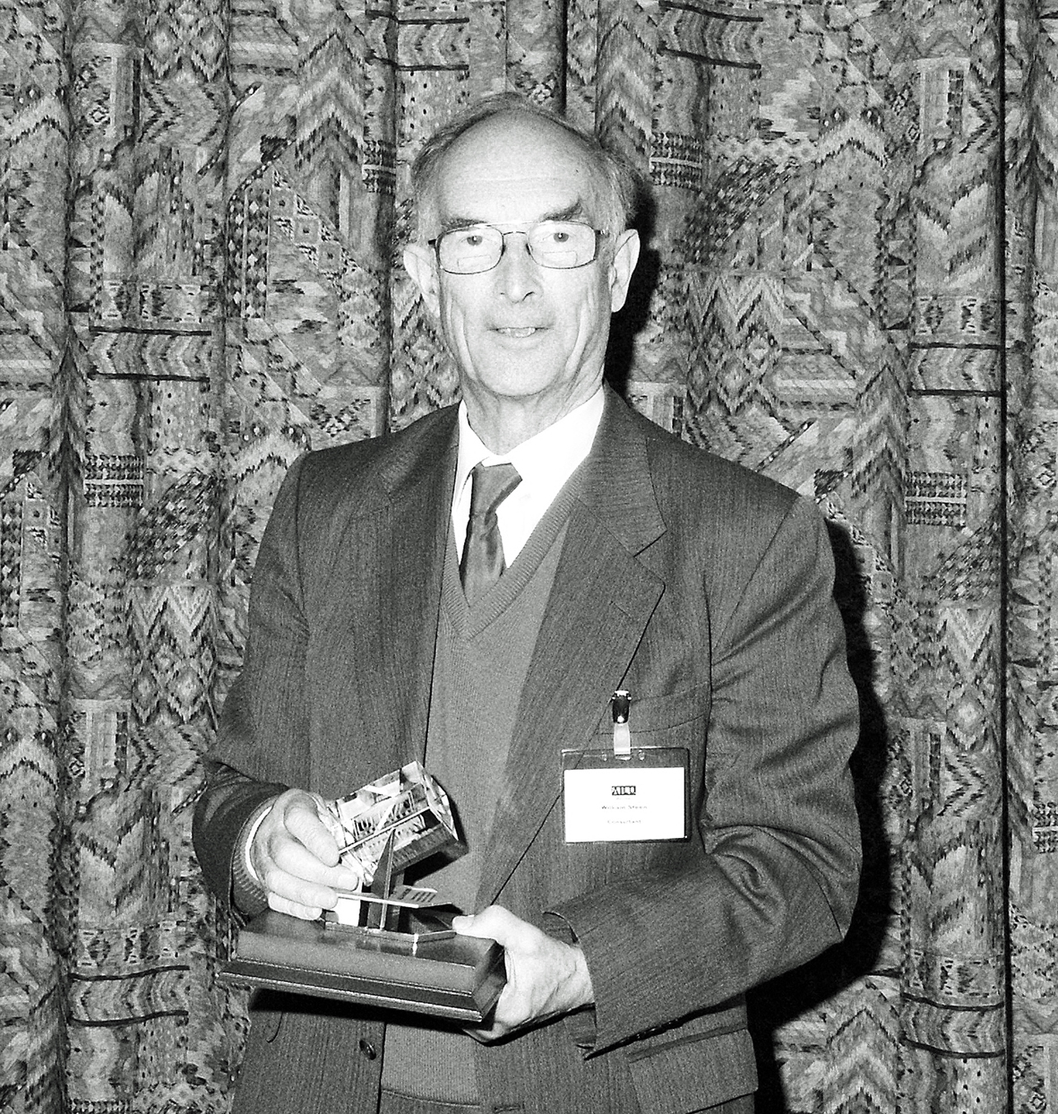
Similarly, the esteemed Professor William Steen presented his speech “The Coming of the Age of Optical Engineering” during the biomedical conference, alongside Fraunhofer Institute of Laser Technology (ILT)’s Dr. Nadine Nottrodt who spoke on “Laser in Biofabrication – How Laser Technology Can Help to Build Artificial Tissue.” They were joined by Dr. Chris Bashur of the Florida Institute of Technology who elaborated on the “Photonic Needs in Regenerative Medicine.”
Participants from the microelectronics industry mulled over the words of Dr. Kumar Patel of Pranalytica Inc. during his plenary speech on “Recapturing the Excitement of High Power Infrared Lasers,” while Dr. Markus Arendt of SUSS MicroTec Photonic Systems spoke on the “Excimer Laser Ablation for High-Density Routing in Advanced Packaging.”
During the automotive-focused conference, Ethan Sprague from the University of Michigan presented his thoughts on “Laser Aided Manufacturing: Atom to Automobile” before Dr. Ted Reutzel of Pennsylvania State University described the “Progress Towards Sensing and Mitigating Flaw Formation in Powder Bed Fusion Additive Manufacturing.” Their presentations joined the observations on “Bottoms Up Digital Design: The Quiet Revolution of the Additive Manufacturing Age” by Dr. Jason Carroll of Eaton, a power-management company that provides energy-efficient solutions to managing electrical, hydraulic, and mechanical power.
To view the highlighted content from ICALEO 2019, including recorded interviews, panels, and speeches, follow LIA’s social media profiles on Facebook, Twitter, and LinkedIn. The 39th ICALEO will be held at the McCormick Place Convention Center in Chicago, Illinois USA from Oct 19, 2020–Oct 22, 2020. Call for papers and Tradeshow booth bookings will be made available soon, and interested parties may contact icaleo@lia.org for further information.
ORLANDO, Fla., Sept. 30, 2019 /PRNewswire-PRWeb/ — Laser industry professionals from academic and industrial settings will be meeting in Orlando, Florida for the 38th annual International Congress on Applications of Lasers & Electro-Optics (ICALEO) conference from Oct 7, 2019–Oct 10, 2019. Organized by The Laser Institute (LIA), the revamped iteration features the four industry foci of Aerospace, Biomedical, Microelectronics, and Automotive.
This year’s ICALEO will introduce a new Business Conference that addresses laser end-users while presenting solutions to challenges that various manufacturing industries are experiencing. A complement to the Technical Conference and its workshops, the Business Conference will allow manufacturers, integrators, and suppliers to selectively engage in the discussion on the unique challenges and revolutionary applications for advanced laser materials processing.
Co-chairs Klaus Löffler of TRUMPF Laser- und Systemtechnik GmbH, and Dr. Henrikki Pantsar from TRUMPF Inc. describe the event as an opportunity to bridge manufacturing and applied research, as well as a platform to highlight laser providers with leading solutions. The exhibitors that attendees will have the opportunity to engage with during the Trade Show include TRUMPF, II-VI, NASA, IPG Photonics, Han’s Laser, and more.
In addition to the Trade Show that will go on across the four days of the conference, conversations will also revolve around the business plenary addresses from the likes of Dr. Christoph Leyens. The Director of the Fraunhofer Institute for Material and Beam Technology in Dresden, Dr. Leyens will speak on the innovative aerospace and space structures made by additive manufacturing during the Aerospace Business Conference day on Oct 7.
He will be joined by Dave Hudson, the President and CEO of Joining Industries and the head of three manufacturing subsidiaries that specialize in different categories of laser-based manufacturing. Mr. Hudson’s presentation will revolve around the expanding use of industrial lasers in aerospace manufacturing.
During the Biomedical Business Conference day on Oct 8, Professor William Steen, the ‘Father of Laser Materials Processing’ and namesake of the inaugural William M. Steen Award will be in attendance to present his talk on the coming of the age of optical engineering. A plenary speech by Dr. Chris Bashur of Florida Institute of Technology will also enlighten the audience on the lasers and optics applications in regenerative medicine.
Dr. Markus Arendt, the President of SUSS MicroTec Photonic Systems, will then elaborate on the practicality of excimer laser ablation for high-density routing in advanced packaging during the Microelectronics Business Conference day on Oct 9.
On the next day, the University of Michigan’s Dr. Jyoti Mazumder will present his plenary address “Laser Aided Manufacturing: Atom to Automobile” for the Automotive Business Conference day. Dr. Jason Carroll, the Global Technology Director for Materials and Manufacturing at Eaton, will follow with his thoughts on the bottom-up digital design for additive manufacturing.
U.S. Department of Labor
Occupational Safety and Health Administration
Office of Communications
Washington, D.C.
Contact: Office of Communications
Phone: 202-693-1999 www.osha.gov
U.S. Department of Labor Approves New Respirator Fit Testing Protocols to Protect Workers from Airborne Contaminants
WASHINGTON, DC – The U.S. Department of Labor’s Occupational Safety and Health Administration (OSHA) today issued a final rule that provides employers with two new fit testing protocols for ensuring that employees’ respirators fit properly.
The new protocols are the modified ambient aerosol condensation nuclei counter (CNC) quantitative fit testing protocol for full-facepiece and half-mask elastomeric respirators, and the modified ambient aerosol CNC quantitative fit testing protocol for filtering facepiece respirators. Both protocols are variations of the original OSHA-approved ambient aerosol CNC protocol, but have fewer test exercises, shorter exercise duration, and a more streamlined sampling sequence.
These two quantitative methods add to the four existing in Appendix A of OSHA’s Respiratory Protection Standard, which contains mandatory respirator fit-testing protocols that employers must choose from to protect employees from hazardous airborne contaminants. The rule does not require employers in general industries, shipyard employment, and construction to update or replace their current fit testing methods, and does not impose additional costs.
The rule becomes effective September 26, 2019.
Under the Occupational Safety and Health Act of 1970, employers are responsible for providing safe and healthful workplaces for their employees. OSHA’s role is to help ensure these conditions for America’s working men and women by setting and enforcing standards, and providing training, education and assistance. For more information, visit www.osha.gov.
The mission of the Department of Labor is to foster, promote, and develop the welfare of the wage earners, job seekers, and retirees of the United States; improve working conditions; advance opportunities for profitable employment; and assure work-related benefits and rights.
# # #
U.S. Department of Labor news materials are accessible at http://www.dol.gov. The Department’s Reasonable Accommodation Resource Center converts departmental information and documents into alternative formats, which include Braille and large print. For alternative format requests, please contact the Department at (202) 693-7828 (voice) or (800) 877-8339 (federal relay).
The Future of Interaction & the Laser Processing Challenges that Stand in the Way
by William S. Land, II, Business Development Manager for Aerotech
As everyone who is interested in display technology is aware, the switch over from LCD technology to OLED displays has begun in the handheld electronics market. However, with technology change and consumer benefit come challenges in manufacturing. As with all production processes, OLED display manufacturers are concerned with yield and production rate. Demand is surging, and the end markets OLED displays supply are time sensitive and high pressure. Some of the major manufacturing challenges related to OLED display fabrication stem from the need for individual component displays to be cut out by a laser. These challenges all come down to three things: displays are getting bigger, they need to be cut very fast because they are too expensive, and most importantly, the materials used to make them are extremely sensitive to process parameters and difficult to cut with quality.
Firstly, handheld electronic displays are trending larger. This poses a major problem for the laser processing of LED based displays. The cutting of individual component displays relies on galvanometer-based laser scanners to achieve economically viable throughput rates. However, there are serious limitations that prevent the manufacture of displays much larger than 100 mm in length by scanner alone. It turns out that OLED display polymers, as mentioned, are very sensitive to laser parameter variations. Therefore, they require specific laser spot sizes to produce high quality cuts. Since laser spot size is directly tied to available working area in galvo scanner systems, this poses a major issue to OLED manufacturers. Manufacturers need the speed of a galvo, but are limited in the field size they can achieve due to laser spot size. Market demand for LED-based displays began in the wearable device market where the constraint on laser scanner working area was less of a hindrance due to smaller device sizes. With mobile and tablet displays trending larger, and adjacent markets such as the automotive industry asking for larger displays, manufacturers are finding ways to maintain the throughput of a scanner-based system while achieving larger working areas.
Image: Multi-scanner system utilizing the IFOV A3200 controller feature to make complex, large-scale, high-dynamic laser processing between multiple axes easy to the user.
The primary way OLED display manufacturers are extending the working area of their laser cutting systems is by combining scanner motion with the simultaneous motion of a larger subsystem. Only a few modern motion controllers allow for this type of synchronization between scanner and servo stage motion in the performance of a single laser path. Manufacturers are using this, what I call a cascaded motion process, to achieve the required scanner-level dynamic performance and speed over a much larger travel range. The cascaded motion eliminates the dependency of scanner field-of-view and laser spot size. This allows process engineers to select the optics best suited to achieve high-quality material processing, independent of the component size the machine will process. Without a combined-motion laser delivery system, it is difficult for display manufacturers to achieve the levels of throughput and yield rates that are required to remain economically viable. As such, this type of synchronized motion is seen as a key enabler moving forward while manufacturers begin to tackle the production of more exotic displays.
An added benefit of controlling the scanner and servo stages from a unified software and hardware platform is the ability to mitigate servo stage dynamic error. Performing the cascaded motion in a single integrated control algorithm allows the scanner to compensate for servo stage tracking errors in real-time. In this manner, LED display manufacturers suffer little to no accuracy penalty over a pure scanner system. This is critical to the process, because maintaining accuracy while processing as fast as possible is another major challenge to cutting component OLED displays with a laser.
The cutting of LED display component assemblies demands high levels of laser spot tracking accuracy through complex geometries. In order to bring cost down as much as possible, individual displays are being laser cut at speeds upwards of 2-5 m/s while maintaining <2-3 µm of peak dynamic accuracy. This level of dynamic accuracy is demanded by the many connections and fine features at the edges of the displays that connect them to the display electronics. Hitting these accuracy tolerances at the required throughput rates is a very difficult motion control task, and added dynamic error from the larger servo stages would eat into the already thin error margins if they were not accounted for through an integrated controls approach to the cascaded motion. Even with the integrated cascaded motion, nearly every modern controls technique must be employed to successfully achieve these specifications. This ties into the most difficult challenge with regard to the laser cutting of OLED displays – the sensitivity of the complex material stacks used to make them.
Traditional laser control techniques are based in the temporal domain. Most pulsed and short pulsed lasers, popular in display manufacturing, are fired at a fixed frequency. As a result, the acceleration that’s required to maintain dynamic accuracy during complex profile segments causes variations in the average fluency and power density delivered to the part. As the laser spot travels through a cornering move where it must slow, laser pulses bunch together causing overheating and poor cut qualities of the display polymers (Figure 1). This is untenable for yield; control over the average path fluency must be maintained with these polymers. The only acceptable option left with traditional temporal laser control is to maintain constant velocity through the entire motion path. Since the maximum velocity has to be constrained to achieve the required dynamic accuracy through the highest dynamic move, throughput is reduced during less dynamic moves. This too is untenable but for throughput. For these reasons, some display manufacturers are moving to controllers that offer the ability to control lasers in unique ways.
Figure 1: An example of temporal versus spatial domain laser control.
One approach to mitigating laser parameter variations caused by acceleration is performing spatial domain pulsing. Spatial-based laser controls enable the user to command pulses as a function of distance traveled by the laser spot rather than elapsed time. By integrating the motion system’s feedback into the laser pulse generator, modern controllers are able to modulate the pulse frequency as a function of the laser spot’s velocity. This maintains constant pulse spacing and therefore average fluency to the part. Through this functionality, a complete suite of trajectory planning and complex motion controls can be applied to the motion system without compromising the quality and yield of cutting operations. This allows for maximum cutting throughput while maintaining stringent accuracy requirements at the high yield rates required by display industry economics.
Other spatial domain laser controls that further empower the user to control energy delivery exist and are frequently used in the cutting of sensitive materials such as LED display components. One example is the ability to modulate average laser power, or pulse energy in the case of pulsed lasers, as a function of position within the optical field of scanner systems. Regulating pulse energy as a function of position can be used to correct for predictable variations in fluency that result from laser spot distortions attributable to the optics. These optical influences are theoretically modeled and can be effectively mitigated by varying pulse energy as the spot diameter increases and decreases during scanner travel. Likewise, integrated knowledge of the entire motion system’s feedback allows for the pulse energy or average laser power to be varied as a function of the tool-on-part velocity of the laser spot. Through modern laser control features such as these, further implicit control over the fluency and power density imparted to the cut path is afforded to the user. The advantages these laser controls offer, however, is largely predicated on a singular control architecture where all feedback signals can be interrogated and combined within the controller. A unified control architecture is particularly key when using such laser controls with combined motion systems such as the cascaded motion approach critical to OLED manufacturing as described above.
As many of the laser control techniques have only newly been introduced to the space of ultra-short pulse lasers, close relationships between motion suppliers and laser source suppliers are being forged to better empower display manufacturers. These relationships are necessary to deliver the most capable combined laser and motion processing system possible to display manufacturers. As the industry progresses into adjacent and more complicated product markets, such as the automotive industry, the continued development of enabling and novel control capabilities between laser and motion will certainly be required. As an example, it is likely that cascaded, coordinated motion and spatial domain triggering will be required in full 3D space to process and cut displays of free-form shape. As flexible and curved LED displays continue to proliferate in everyday life, modern control features such as those discussed will help to open new LED display markets. To learn more about how Aerotech is already driving innovation in the display market with advanced motion and laser control features, or how we might improve your LED manufacturing capabilities, give us a call.
This article was written by William S. Land, II, Business Development Manager for Aerotech, Pittsburgh, PA. Will started his career at Aerotech in 2011 as a mechanical development engineer and has since served in various positions in engineering, product management and business development roles. Will holds a bachelor’s degree in mechanical engineering from Penn State University and a master’s degree in mechanical engineering from the University of North Carolina at Charlotte. He is currently pursuing an MBA at the University of Pittsburgh.
The LIA has introduced a set of annual awards dedicated to Professor William Maxwell Steen, a veteran and pioneer of laser technology.
This year the Laser Institute (LIA) announced a new set of awards that it plans to confer annually to user organisations that demonstrate significant innovation in the use of lasers for advanced materials processing. Finalists and recipients of the awards will present their innovations at the International Congress on Applications of Lasers & Electro-Optics (ICALEO) on 7-10 October.
The awards will be conferred across each of the following industries: aerospace; automotive; medical devices; microelectronics; specialised manufacturing and services; research and development; life sciences; defense; academic and public sector.
They are dedicated to Professor William Maxwell Steen, a pioneer of laser materials processing research who is commonly referred to as ‘the father of laser materials processing’ in the industrial laser community.
Steen, in addition to founding the world’s first university-based research group in laser material processing at Imperial College London in 1968, can be accredited with the invention of laser chemical vapour deposition, laser arc hybrid welding, and with his research group, the development of blown powder laser cladding and laser direct casting – processes which formed the foundation of laser additive manufacturing for metallic materials, more commonly known today as 3D printing.
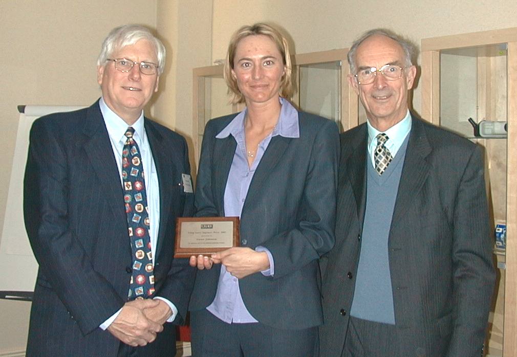
Emma Johnston being presented with the AILU Young Engineer’s Prize by John Bishop (left) and Professor Steen, who was Emma’s PhD supervisor at Liverpool University and AILU president at the time
He also co-founded the Association of Industrial Laser Users (AILU) in 1995 and served as its president for the first eight years. In addition, in 1997 Steen was the first European to be awarded the Arthur Schawlow Award by LIA, and at ICALEO 2008 there was a tribute session to his lifetime achievements. He has a laboratory named after him at the University of Vigo, Spain, and has received a medal from Pelacky University in Oloumouc, Czech Republic, for his pioneering work on lasers.
Steen’s textbook Laser Material Processing – the fourth edition of which was published in 2010 – has for years been a vital source of information for students, researchers and engineers learning laser material processing. Many of Steen’s ex-students (and even their ex-students) now either run their own business, teach, or make money from laser material processing.
On hearing the announcement of the new award, Laser Systems Europe approached Steen to find out more about his many experiences exploring the realm of laser technology.
When did you first begin working in laser technology?
In 1964 I was appointed lecturer at Imperial College London in process metallurgy. I became interested in metal extraction by volatile compounds, such as chlorides, and this led to trying to make patterns by depositing metal from volatile compounds, such as nickel carbonyl. I realized that the pattern created using shaped jets on hot plates was very blurred, and thus needed to make a shaped hot spot. I bought a glass tube with mirror mounts from Ealing Scientific, built my own power supply and I had a very unstable 5W CO2 laser on which I invented the process of laser chemical vapour deposition (LCVD), which worked but obviously needed more power.
In working this up I won a contract for the first industrial fast axial flow 2kW CO2 laser from BOC developed by The Welding Institute (TWI). That gave me the most powerful university-based laser in the UK. Students and contracts flowed from this with the wide-open space for research using this entirely new form of industrial energy.
As a pioneer of laser technology for industrial materials processing, how has industry’s view of laser technology changed?
The very early years were dominated by numerous small start-up laser companies wishing to sell their lasers and compete to find useful applications at sensible prices, this was the main challenge – a solution looking for a problem. Cutting and welding were the only applications at that time with some curious results.
Martin Adams, at TWI, was publishing cutting figures significantly better than everyone else, but because of the atmosphere of competition, this was explained as commercial optimism. Later we came to realise he was able to cut nearly twice as fast as others because TWI had not the space for the cutting table other than in line with the laser, and the beam polarisation favoured his layout as opposed to those with transverse tables; a feature of optical energy not fully understood in those exciting times. There were many more surprises to be found as we explored this new form of energy!
For the next 20 years or so, the reliability and ease of maintenance of lasers improved, with most industries keeping a watching brief on what was going on. I felt at the time I could go to any company and sell the idea of a laser application as a result of this interest.
In the 1990s the fibre laser arrived on the scene and the game changed. The fibre laser was smaller, required less cooling, had no alignment problems and a superb loworder mode beam. To some extent it was like a dream come true.
Today, reliability and quality are taken for granted, and the only thing holding the laser back now is cost, which is rapidly coming down as more units are required. It used to be good to see the look of awe on people’s faces when you said you worked with lasers, now it is not really regarded as unusual. In summary, the opinion of industrialists today is that the laser has arrived, and they are learning to live and work with it.
Are there any particular applications of laser technology you’ve enjoyed watching develop since your retirement in 1998?
There are many applications I have enjoyed working on, but additive manufacturing comes immediately to mind as something special – a game changer in the thinking of how to make things. In the 1980s Rolls Royce asked us to blow powder into the laser beam and so we invented the laser cladding process. It worked
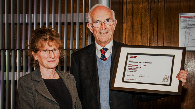
Professor Steen being presented with an Honorary Fellowship to the Institution of Mechanical Engineers by the institute’s president Carolyn Griffiths
so well it became similar to writing with metal, then one day one of my students, Mark McLean, repeatedly overlaid a clad line and produced a wall. One look at that wall, particularly after a metallurgical examination showed the columnar grains running up the wall instead of across the wall – as in a standard casting – showed that we had a serious new manufacturing process on our hands.
Mark went onto make a stainless-steel wine glass, and additive manufacturing was born. Students of mine over the world have now worked on this promising development.
I watch with both amazement and joy at the ingenuity of what is being done with additive manufacturing, and await the day that someone makes a hand-held device, either wire or powder-fed whereby the craft community can actually sculpt in reverse – building things up instead of chiselling material away. The precision is such that in the hands of a craftsman, stunning works of art would be created. If the price is right there would be a huge market for such equipment.
Are you satisfied with how university laser research groups around the world are interacting and collaborating?
There is quite a network of friends among my ex-students based at various institutes around the world who have a strong collaboration, while still remaining competitive, which is as it should be.
One of my main concerns is the lack of imagination at universities. It is obvious to me and others working with lasers that they are dealing with an unusual and highly flexible form of energy available in a uniquely controllable form which can be of almost unlimited power, from milliwatts to petawatts, deliverable in times ranging from continuous to femtoseconds or even less, over a huge range of wavelengths.
The applications of this energy range from material processing through to sensing, metrology, communications, medicine, fluorescence, interferometry, holography and x-rays. This is far more than electricity has to offer, and yet there are currently very few or no university departments dedicated to optical energy – amazing!
Could you give an example from you career where academia has interacted well with industry?
One of our most successful developments came from the work of Professor Lin Li – a past president of LIA and AILU now at Manchester University – who while exploring the possibility of sealing concrete by surface melting – for ease of cleaning, sterility etc – found that thermal cracking made this difficult.
In expanding the beam to try and avoid this he found that he could explosively remove the top centimetre of the surface in reasonably large lumps. Such a simple process was taken up by British Nuclear Fuels (BNFL) for scabbling the walls of radioactive tanks prior to decommissioning. Lin Li proved the process worked and BNFL developed it further at TWI and finally used it for real in their works.
This initiative of the LIA in instituting annual awards for the best developments coming from industry or universities should further enhance academia’s connectivity with industry, and it is very flattering that the LIA has named these awards after me!
Do you have any pearls of wisdom for those looking to start their own entrepreneurial laser journey?
It is certainly stimulating to watch my students set up a business. Those that succeed either need good financial backing and/or a great determination to win. For example, Dr John Powell started Laser Expertise in Nottingham with two friends, they were young, energetic and disciplined in work habits and finance. They spent within their budget by buying a second-hand laser and worked several years for very little return while they expanded the business of a laser job shop. John had a partner for finance, a partner for sales, and he himself had a talent for invention and much more. Together the three of them made a success of the company, which I believe now employs some 60 people.
So, if there is any pearl of wisdom, it is to have a belief in yourself and a determination to win, even when the going is tough. In the laser business the rewards can be great, with much excitement and potential novelty at any time.
A full version of this interview can be found online at www.lasersystemseurope.com