The Liège company, LASEA, is raising equity capital of over 6 million euros from its historical shareholders.

Liège, 7/10/2019 – LASEA, one of the world leaders in laser micromachining, has announced
it is tripling its equity and entering a new growth phase in its various markets. The current
shareholders (Epimède, SRIW, Noshaq and private shareholders) are backing this operation to
the tune of 6.1 million euros (first phase) to which will be added almost 10 million euros thanks
to additional support from Europe and the Walloon Region.

LASEA, the high-tech Liège company, a laser micromachining pioneer

With annual organic growth of 32% since 2012, in 7 years, LASEA has multiplied its revenue and its
workforce by 7. Now the European leader of femtosecond laser micromachining, it is rapidly
increasing its market shares in the USA and Japan.

LASEA machines are used for cutting, marking and texturing materials with unrivalled quality and
precision (up to 0.2μm, i.e. 250x smaller than the width of a human hair). With cutting-edge R&D at
the international level, it regularly initiates innovations well in advance of the state of the art (cutting
with no conicity, bio-mimicry, machining along 7 axes simultaneously, etc.).

The capital increase will bolster its growth of recent years in both its primary sectors (pharmaceutical
industry, luxury, medical devices) and in new sectors like electronics.


New resources to accelerate its growth further and develop new sectors

LASEA S.A. l Liège Science Park l Rue des Chasseurs Ardennais 10 l 4031 Angleur l BELGIQUE 2 / 3
“With this capital-raising operation, the biggest since LASEA was founded, we are giving ourselves the
means to match our ambitions. Our strategy is to further strengthen our commercial presence in our
various countries while pursuing our cutting-edge technological developments in laser micromachining.

To achieve our goals, we are going to extend our campaigns to recruit new talent and to seek synergies
with other companies in our market niches”, Axl Kupisiewicz, Lasea CEO stated.

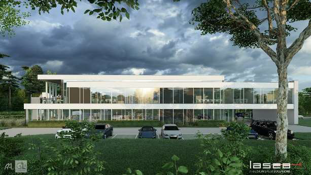
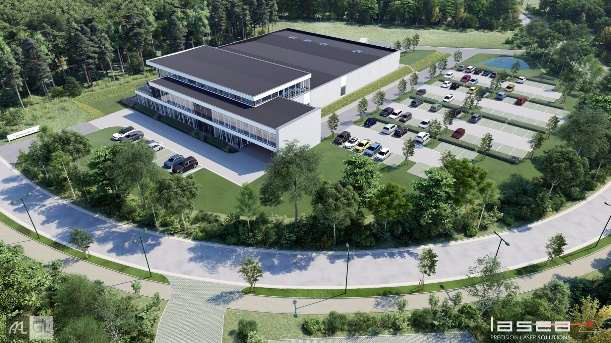
To support this new development phase, a new building in the Liège Science Park will come on-stream in
June 2020. The 4,000 m² of office and production space (workshops and clean rooms) will allow the
current production capacity to be multiplied by three. This investment is covered by a loan of 7 million
euros from BNP Paribas Fortis and Belfius.

Benoît Fellin, Investment Manager at the Noshaq Group: “We have backed LASEA in all its development
stages, since it was founded in 1999. Today, and starting at Liège, LASEA is acknowledged internationally
for its very specific expertise. We are therefore very enthusiastic about taking part in this operation.
These new resources will allow LASEA to continue to grow.”

Pierre Paraire, responsible for handling the matter at SRIW: “The entrepreneurial ability of the founder,
an innovation strategy translated into a product strategy, international deployment, the level of
qualification of human resources, etc. All these factors have led SRIW to reaffirming its shareholder’s
support for LASEA by taking part in this new capital-raising operation”
Philippe Degeer, Investment Manager at Epimède: “We are delighted once again to have established a
partnership with LASEA and other key investment funds to support this ambitious growth project. Our
goal is to help the company grow and enable it to reach a higher level. We have full confidence in the
ability of the LASEA team to offer exceptional performance in the future and are delighted to be part of
this project.”

The equity capital-raising operation will allow the company to initiate a new development phase, to
accelerate sales and to continue a process of industrializing new products stemming from its major
research programs.
These new resources will be used to:

  • Expand the sales and marketing force
  • Develop the subsidiaries (Bordeaux – France; Biel – Switzerland; San Diego – USA), as well as the
    new agents’ and distributors’ network (Japan, Australia, United Kingdom, Netherlands, Spain,
    Germany, Taiwan, etc.).
  • Hire new talent to finalise the new products targeted at the medical and electronics sectors
  • Strengthen synergies with companies in its market niches
  • Promote 2 new softwares worldwide (deployment in January 2020)


About LASEA:
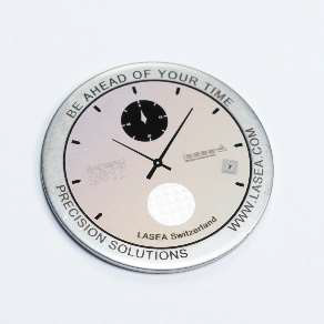
Founded in 1999, LASEA supplies production lines to the most prestigious companies in the world
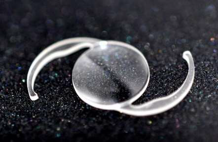
including the top 3 Swiss watchmakers, leading glasses manufacturers, the pharmaceutical and medical
industry (intra-ocular and cochlear implants), as well as several big names of Silicon Valley. Active in 27
countries and on 4 continents, it has already installed more than 300 machines worldwide (production
systems and lines operating 24 hours a day). In addition to its headquarters in Belgium (Liège Science
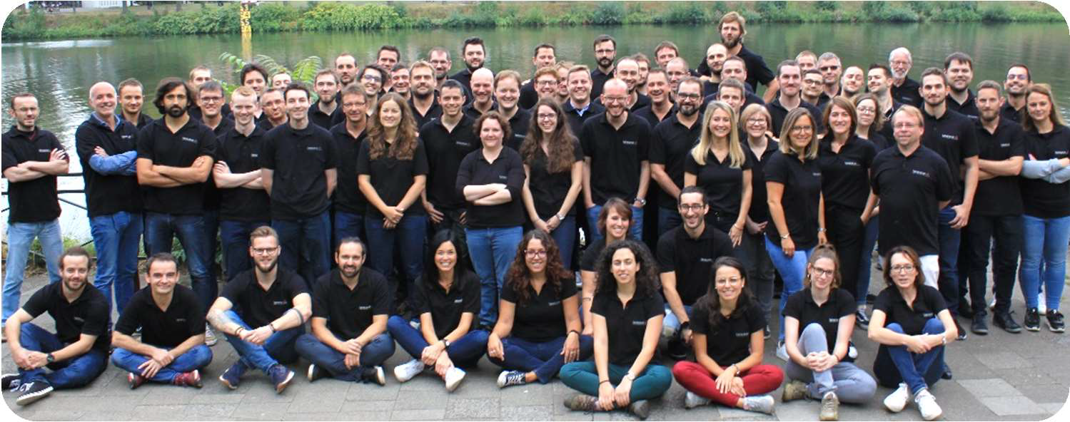
Park), it has subsidiaries in Bordeaux, San Diego and Biel. It employs 80 people and owns a 25% stake in
CISEO (formerly WOW group) with CITIUS and UNISENSOR.

LASEA has been a finalist in the competition of the Promising Enterprise of the Year (EY), is part of the
50 fastest-growing companies in Belgium (Fast 50 – Deloitte) and has won various awards including the
Wallonia Export Grand Prix 2018 (AWEX) and the Micron d’Or 2018 (Machine-tools
category). www.lasea.com

About Noshaq:
Noshaq is the financial partner of reference for the creation and development of SMEs in the Liège
region. Over the years, Noshaq has developed a panel of funding vehicles in line with market needs and
trends and with its strategy. www.noshaq.be

About SRIW:
S.R.I.W. develops a wide range of customised solutions to support business creation, development
through innovation or investment, internal and external growth, the creation of subsidiaries in Wallonia,
Belgium or abroad, winning new markets, etc. The value of its shareholdings currently exceeds 2.2 billion
euros. www.sriw.be

About Epimède:
Epimède Capital is an investment fund targeting small and medium-sized enterprises with high growth
potential in the technology sector. www.epimede.com

Contact
Violette Marbehant – Marketing Account Manager
vmarbehant@lasea.com +32 4 365 02 43 / +32 497 43 46 63

Laser Micromachining of Transparent Dielectrics – Glass and Quartz Using Nano Short Pulsed Nd: YVO4 Laser Harmonics

By Shiva Gadag, Radovan  Kovacevic and Nilesh  Ramani

Introduction:
Glass, Quartz, and Silicon are made out of sand grains consisting of Silica, SiO2. Silicon and Glass are two basic building blocks which go hand-in-hand in the fabrication of optoelectronics and microelectronics device for MEMS and Biomedical microdevice applications such as charge coupled device, lab-on-a-chip, microsensors, microfluidic arrays, PV solar cells etc.

Miniaturization of microelectronics device is the driving force for laser micromachining of transparent dielectric Glass, Quartz and semiconductor Silicon materials. The dawn of digital era has diminished the dimensions of digital devices to micron and submicron scale resulting in shrinking the size of silicon and its dioxide dielectrics based digital devices much faster than the predicted ones by the Moore’s Law. In order to meet the digital demands of the 21st century digital revolution, laser micromachining or laser lithography is the only workhorse for alternative noncontact toolless techniques for digital device micro-manufacturing. Laser micromachining with shorter pulse widths result in accurate spatial resolution, precise depth control, enhanced edge quality and minimal peripheral damage. On the other hand conventional mechanical machining of transparent dielectrics and semiconductors is economically expensive and time consuming due to the hardness and brittleness of these materials. Nano short pulses and Ultrashort pulses are most commonly used for micromachining of transparent materials. The microprocessing of hard and brittle transparent materials is accomplished due thermal ablation by heating and evaporation of surface atoms in the former laser process. The nanosecond laser micromachining can often induce some undesirable heat affected zone surrounding the feature. Whereas in the latter process, the photoablation directly results in material vaporization by breaking the atomic bond by stripping electrons. The ultrashort micromachining is cold ablation with negligible heat affected zone due to no heat transfer to surrounding area. However, ultrashort micromachining techniques are quite expensive for industrial processing of glass such as cutting, drilling and marking for touch screen glass panel displays, microfluidic chambers, solar panels and microlens and optical components for photonics industries. As a result ultrashort processing is ideal only for applications demanding extreme precisions and excellent quality with negligible HAZ. However, a similar precision and quality of micromachining of transparent, hard and brittle materials can be achieved with nanosecond short pulsed lasers but with some traces of HAZ. The nano short pulsed lasers are relatively less expensive as compared to ultrashort lasers but far more efficient than the conventional machining methods. Hence the purpose of this article is to demonstrate the ease and efficacy, pros and cons of nanoshort pulsed lasers in micromachining of transparent and brittle materials like glass and quartz using Nd: YVO4 laser harmonics.

Experimental Technique:
The micromachining system (Figure-1) used nanosecond pulses (11ns duration) of Nd:YVO4, DPSS, Q-switched, HIPPO laser with four harmonics generating fundamental IR λ=1064nm, 2) Green λ=532nm, 3) UV λ=355nm and 4) UV λ=266nm respectively. The micromachining gantry consisted of X,Y,Z stage with laser mounted on the top tier was focused after 8X beam expansion by

Figure 1 – Laser micromachining work stage (left) and experimental setup (right) to measure laser power transmittance in glass.

telescopic lens and 90o reflections by 2 mirrors on incoming beam opening of HurryScan-II. The scanner focused beam to diffraction limited spot diameter, d=18 microns using 100mm telecentric lens and rastered beam as per CAD feature on substrate view field of 45mm. The substrates were 1mm Corning#0215 glass and 2mm photolithographic Quartz. PerkinElmer LAMBDA UV/Vis/NIR spectrophotometer was used to determine transmittance of glass for the range of wavelengths covering four laser harmonics. Glass being transparent (T>90%) IR and green wavelengths, the first two harmonics are not suitable for micromachining. The absorbance of UV wavelengths being A>75% , the third and fourth harmonics are better suited and fourth harmonic UV λ=266nm is most ideal among the four harmonics for micromachining of glass.

Defect Diagnosis of Dielectrics:

Figure 2 – The defect diagnosis of laser induced cracks showing A) regular cyclic cracks formed by primary mode-I type of precrack, B) regular periodic nodes of Butterfly type of cracks, C) Colony of Crack grain boundary surrounding the vias and D) concentric circles of dentritic debris of droplets of molten glass

Hence UV laser was used for micromachining of glass and quartz but the initial trials with high diode current resulted in various types of defects shown in the Figure 2. Systematic analysis of the defects formed in glass during micromarking and drilling revealed two types of crack formation, namely periodic and irregular type of cracks. The primary mode-I crack formed during marking of parallel lines with high diode current at high repetition rates, propagated as cyclic crack with a well-defined wavelength of propagation all along the length of the parallel lines on glass while micromarking, The cyclic micro cracks formed by primary mode-I crack either propagate as secondary sinusoidal crack with a wavelength of propagation proportional to the wavelength of laser harmonics. Alternatively primary precracks propogate as tertiary transverse cyclic cracks along the transverse line of laser marking with a wavelength equal to perpendicular distance between the parallel lines of laser marking. The second type of periodic cracks appeared as periodic nodes of cracks at regular interval resembling tiny butterfly. The irregular type of cracks formed crack grain boundary during laser drilling of microvias on glass due very high diode currents or pulsing frequency. The irregular cracks formed colonies of cracks surrounding the microvia. The expulsion of molten glass debris often solidified as concentric circles of dendritic glass droplets surrounding the circumference of the micro vias array formed on glass.

Optimum Power, Frequency and Wavelength of Laser:
Apart from the transmittance of various wavelengths in the glass, absorbance of a suitable wavelength and its response to average power and pulsing frequency of the laser is crucial for micromachining of the glass without any defects or cracks. To establish the power and frequency response to absorbance of the laser, average power transmittance characteristics of glass for the laser harmonics were determined using the setup shown in the Figure 1. The diode current of the diode pumped solid state laser is directly proportional to average power of laser harmonics. As the diode current increased from 1 to 100% , the average power laser harmonics linearly increased to 17.5W for IR and 8.5W for Green, 5W for UV λ=355nm and 2.5W for UV λ=266nm respectively. Since absorbance characteristics of laser to diode current and frequency of pulses being identical for all four harmonics, second harmonic green laser λ=532nm was chosen to study the power and frequency response to absorption of the laser.

Intensity, I0 of power incident, P0 on glass in air, I0 = P0/(pr2) and transmitted intensity, IT of power, PT through glass IT= PT/(pr2) were measured by thermopile sensor. Applying Beer-Lambert’s law due to high optical penetration of the glass, absorption coefficient of the laser in glass thickness, l was calculated using b =-ln(IT/I0)/l . Diode current and frequency response of laser absorption in Corning glass measurement (Figure 3) indicated optimal laser power for 60-70% diode current and frequency of 55 kHz for effective micromachining.

Figure 3 – Measurement of absorption coefficient of Corning glass as function of A) Diode Current and B) Pulsing Frequency (kHz) of HIPPO Laser.

Results:
Finally using the suitable wavelength (λ=266nm) and optimal energy (5-10 µJ) and frequency (50 kHz) of 11ns short pulsed UV laser, cracks were eliminated and defects were minimized in micromachining of glass. The process optimization enabled to get fine parallel lines of 17µm and arrays of microvia of 15µm diameter at 75µm pitch, as well as etching and scribing without any cracks on glass (Figure 4). This helped to make microchannels and microfluidic tubes in 2mm thick quartz using nanosecond pulsed UV laser.

Figure 4 – Optimization of laser parameters enabled crack-free micromachining of glass: A, B) Fine line marking, C) drilling of microvias, and D) etching and scribing of glass.

Conclusion:
An optimization of laser process parameters – wavelength, power and frequency nanosecond pulse laser crucial critical factor for micromachining of transparent dielectrics of glass and quartz with minimal HAZ, less defects and relatively free from flaws and cracks. The technical feasibility of the cost effective nanosecond pulsed lasers in microprocessing of transparent dielectrics is clearly established in this article.

Professor Radovan Kovacevic is with Dept. of Mechanical Engineering, Southern Methodist University, Dallas TX and Shiva Gadag is with ScanTech Lasers Pvt. Ltd. Nilesh Ramani is Director & CEO of Scantech Laser Pvt Ltd, India.

Laser Micromachining RF Antennas for Contactless Payments

By Debbie Sniderman

Contactless methods are next in the evolution of consumer payment options. Physical contact was needed to integrate payment cards with point-of-sale terminals using magnetic stripes or chips. The faster tap-and-go contactless interactions using Radio Frequency (RF) communication and inductive coupling with a card reader are becoming more widespread. They’re more convenient, more secure, and can link to many different types of payment systems such as subways to help reduce the need for cash.

Typical payment cards with both contact and contactless interfaces have two types of antennas, one on the back of the card’s communication chip (IC) and a separate booster antenna on the card spanning its entire body. This larger antenna helps the passive system harvest enough power from the electromagnetic field when it is within the working range (~4 cm) of the card reader.

Traditionally antennas on plastic cards are created with wire windings or lithography and batch chemical etches when produced in high volumes. But, Alan Conneely, Centre Manager at the National Centre for Laser Applications (NCLA) at the National University of Ireland Galway, says high resolution UV nanosecond laser ablation techniques and new antenna designs have allowed the creation of IC antennas without booster antennas.

UV nanosecond laser ablating antennas from ½ oz copper printed circuit board materials

His group’s new techniques offer many production advantages, but also increased card reliability. “The coil on module technology eliminates the need for the interconnection to the chip as it uses a second RF induction loop. When it is bent in a wallet, it doesn’t break as easily. It is more self-contained,” says Conneely.

Schematic showing how a card reader (left) inductively couples with a coil on module contactless payment card (right) through its secondary antenna module for power harvesting and communication

Ablation Processing
Together with industry partner AmaTech Group Ltd, and the Antenna & High Frequency Research Centre at the Dublin Institute of Technology, Conneely’s team created IC antennas with optimized designs and laser ablation processing suitable for use without booster antennas. They performed RF modeling and simulation, antenna design, laser ablation processing trials on copper PCBs and testing to optimize the following process and quality goals:

  • Complete electrical isolation with minimal debris within ablated kerf
  • Narrow kerf to enable increased resolution
  • Minimal heat affected zone to avoid damaging electrical track
  • Minimal damage to FR4 substrate to ensure long-term antenna robustness and prevent copper layer delamination

Process parameters such as power, repetition rate, pulse energy, scan speed, number of passes, antenna tool path length and cycle time were varied. Devices were produced and tested to check performance and processing relationships.

Smaller Antenna Resolutions Possible than Chemical Etch
Conneely says the resulting devices demonstrated robust isolation and minimal substrate damage. In addition, one key advantage to laser ablation processes in the copper thickness tested is it created higher resolution structures compared to other production methods. At 17 µm copper thickness, the smallest chemical etching feature separations are around 75 µm.

The laser ablation studies in this research produced kerf widths in the range of 15-25 µm with an optimal combination of isolation, resolution and throughput. With better resolution machining capabilities, IC antenna designs can have more coil turns per given area.

Laser ablated prototype antenna module with soldered RF transponder chip

Wearable Payment Devices
Europay, MasterCard and Visa (EMV) industry standards exist for contactless cards and payment systems, and they currently are under development for wearable objects. Wearable devices are aiming for an activation distance of 4 cm from the reader for ease of use. In this work, laser ablated antenna modules on flexible substrates were inserted into a wearable wristband with new antenna designs and were able to meet the 4 cm activation distance and other EMV industry standards.

“One challenge lasers have always had to overcome when compared to mass batch production are techniques for high volume production. Improving the antenna designs and using traditional techniques for improving throughput, such as multiple lasers, beam splitting and thinner copper will speed up the process and make the laser ablation process more effective,” says Conneely.

LED representation of the working envelope of where the card would operate in space when over and close to the card reader. Outside of this envelope operation ceases

LED representation of the working envelope of where contactless payment card would operate in space when close to the card reader shown in overlay. Outside of this envelope operation ceases

More Flexible Designs Possible
The industry trend is moving away from cards towards bracelets, key fobs, jewelry and other wearable devices. “As producers move more towards customized wearable designs with smaller batch runs, laser ablation processes will be competitive and very helpful. Laser machining processes are flexible and able to change more quickly than chemical batch etching when antenna design configurations change for any kind of object,” says Conneely.

In addition to designs on plastic substrates, Conneely’s group also has designs for metal substrates which attenuate RF signals that demonstrate better performance. “Metal cards offer greater aesthetic appeal and card feel resulting in higher value payment devices. Higher-end payment cards and wearables such as jewelry would ideally use metal substrates. The laser machining process allows for larger antenna design spaces, more design iterations faster, and overall more opportunities for antenna design,” he says.

“Contactless payment systems are currently a very competitive market. Our technology is still in development, heading towards manufacturing, which involves working not only with the card issuers, but all of the stakeholders in the financial space,” Conneely says. He will present more on this topic at ICALEO, Oct. 16-20, 2016 in San Diego, CA in his talk M501 in the Laser Microprocessing Conference LMF Session 5 on Tuesday.

Debbie Sniderman is a freelance writer for LIA.

Clark-MXR, Inc. – July’s Featured Corporate Member

An industry leader in Ultrashort Pulse laser based micromachining and the production of ultrafast lasers and laser-based solutions for scientific research and industrial applications, Clark-MXR, Inc. is known for offering unparalleled contract manufacturing services and easy-to-use laser products at a low cost of ownership. Located in Dexter, Michigan, Clark-MXR, Inc. serves customers from universities, laboratories and industries across the globe.

Clark-MXR, Inc. was incorporated as a Michigan corporation in 1992, to acquire the assets of two running companies: Clark Instrumentation Inc., founded by Dr. William Clark, and Medox (MXR) Research, Inc., founded by Dr. Philippe Bado – a member of Professor Gerard Mourou’s research group. As the world’s first commercial ultrafast laser company, Clark-MXR, Inc. has introduced many first-to-the-market products since its inception, including its CPA-1000 in 1992. In addition, Clark-MXR, Inc. has been involved in the use of ultrafast lasers for micromachining based on research conducted at Professor Mourou’s laboratory at the University of Michigan.

The company’s products and services stem from its two main divisions: the Laser Products Division and the Micromachining Division. Responsible for designing, building and servicing ultrashort pulse lasers for scientific and industrial applications, the Laser Products Division also manufactures micromachining workstations that are used in industrial micromachining, micro-manufacturing and proof-of-concept process development. Its complete system solutions meet a variety of industry needs, from ultrashort pulse micromachining workstations based on Model CPA-Series Ti:Sapphire lasers to Model IMPULSE, Yb-doped fiber lasers and complete nonlinear spectroscopy systems. Additionally, this division of Clark-MXR, Inc. produces accessories, such as NOPAs and harmonic generators, and offers customized product development, consultation and collaborations.

The formation of the second division, the Micromachining Division, was initiated by the introduction and success of the first commercial ultrafast laser based micromachining workstation in 2002, Model UMW based on Model CPA-Series laser. Providing value-added service to the semiconductor, medical and other high tech industries, this division utilizes the company’s ultrashort pulse lasers to cover a range of tasks, from prototyping to routine part production.

The Micromachining Division consistently meets its goal of addressing the growing demand for micromachined parts using ultrafast lasers, which offer a superior quality when compared to traditional methods. Because of the company’s innovative technology and extensive knowledge from the last 20 years, Clark-MXR, Inc. can machine a wide variety of materials – including ceramics and refractory metals – without recasting, heat-affected-zone (HAZ), delamination or melting. The micromachining technologies utilized within this division of the company can be adapted for innovative research – from 3D tomography and geological sample analysis to laser ablation mass spectrometry and LIBS. With a clearly-honed expertise, state-of-the-art inspection facilities, and a dedication to working closely with customers, Clark-MXR, Inc. develops custom methodologies that successfully fulfill customers’ unique needs.

Over its history, Clark-MXR, Inc. has grown, now earning recognition as a premier company in the laser industry for ultrafast laser micromachining and for its numerous ultrafast laser products, including many first-to-market products and innovations. The range of products and services the company offers today includes Model CPA-Series Ti:Sapphire Ultrafast lasers, Model IMPULSE Yb-doped high power/high energy fiber lasers, Ultrafast Micromachining workstations,  and complete system solutions for micromachining and research sectors, including fully customized systems. In addition to its range of products, Clark-MXR, Inc. works to help the growing ultrafast laser based micromachining industry, among other things, through its Ultrafast Micromachining Handbook, which was introduced in 1999 and is now freely available on the Clark-MXR, Inc. website to familiarize individuals with the novel physics of ultrafast laser based material removal processes.

Since joining Laser Institute of America (LIA) in 1999, Clark-MXR, Inc. and its team have been actively involved in the organization, with Dr. William Clark serving as LIA president in 2005.

For more information, visit www.cmxr.com.

Micromachining Sapphire

UV Nanosecond Lasers Enable Finer Detail

By Jan-Willem Pieterse

CO2 lasers have long been the laser of choice for processing applications due to their power/cost ratio. CO2 lasers in sapphire create a classic melt pool, which can be blown out to achieve a full cut. However, the cut is often too crude for semiconductor applications.

Pulsed UV lasers enable machining with much finer detail, and their lack of excess heat adds another benefit — Each pulse removes a small amount of material but the high repetition rate turns it into a fast process.

Nanosecond Nd:YAG lasers can micromachine sapphire substrates of any shape and a wide variety of thicknesses. A combination of 3D cutting and a galvanometer-scanner system delivers high accuracy and edge smoothness. Continue reading