Graphene – it’s the two-dimensional (2D) allotrope of carbon atoms that ignited the imaginations of researchers across the globe. Heralded as a ‘miracle material’, its potential seemed limitless and it was predicted to usher in the next generation of technology. Flexible, stronger than steel, transparent, lightweight, and an amazing conductor of heat and electricity, it was going to revolutionize everything from household electronics to biomedical nanotechnology.
THE PROBLEM
Yet, nearly eight years after Dr. Andre Geim and Dr. Konstantin Novoselov earned the Nobel Prize in Physics for first isolating graphene and identifying its properties, graphene has encountered barriers to moving out of the lab and into the marketplace. According to Prof. Dr. Aravinda Kar of the University of Central Florida’s Center for Research and Education in Optics and Lasers (CREOL), one of the most prominent barriers has been finding scalable manufacturing processes that can produce graphene of a quality and quantity ready for consumers and businesses.
Graphene is notoriously difficult to synthesize in large quantities at a consistent quality. Early methods of isolating graphene involved a slow and tedious mechanical exfoliation technique; the researchers would extract a thin layer of graphite from a graphite crystal using regular adhesive tape, continually reducing the graphite sample by sticking the tape together and pulling it apart until only a small, 2D section of carbon atoms with a honeycomb lattice remained. Graphene’s unique characteristics are only present when it is one, two, or three layers of atoms thick – any thicker and it becomes graphite, losing all of the exceptional properties of graphene. The tape exfoliation method, although useful for the lab, was not going to translate very well to an industrialized process.
SOLVENT-AIDED EXFOLIATION AND CVD
Two of the more promising and potentially scalable methods of producing graphene are solvent-aided exfoliation and chemical vapor deposition (CVD). In solvent-aided exfoliation, sonication is used to exfoliate graphene crystals which are then further separated in a solvent and later gathered into graphene monolayers. Scientists at the National University of Singapore have identified a flocculation method that reduces the amount of solvent needed for their exfoliation process, which could yield graphene using far less solvent than was previously needed. Another method experiencing innovation is CVD, which uses thermal chemical reactions to ‘grow’ graphene on substrates of specific materials, typically copper or silicon. Recently, engineers at MIT developed a CVD process for producing graphene filtration membrane sheets at 5 cm per minute. One of the biggest issues with traditional CVD and exfoliation methods is the need to transfer graphene from its fabrication platform to a substrate. Lasers are going to change that.
THE MISSING PIECE – LASERS
Lasers may provide yet another avenue to the elusive mass production of graphene, with an eye toward innovating the semiconductor industry. In 2003, Kar, along with Dr. Islam Salama and Dr. Nathaniel Quick, realized that laser direct writing could be used to fabricate carbon-rich nanoribbons on a silicon carbide (SiC) wafer in a nitrogen rich environment. Although these ribbons were too thick to be considered graphene, Kar believed that with a few changes, this process could be reworked to synthesize graphene in situ on a large scale, very quickly. In 2013, Kar and Quick were issued a patent for a Laser Chemical Vapor Deposition (LCVD) method that could be scaled for mass production.
Their method involved a few simple components: a frequency doubled Nd:YAG (green) laser of 532 nm wavelength, methane (CH4) gas, a silicon substrate, and a vacuum chamber.
The 532 nm wavelength corresponds to a photon of energy 2.33 eV, so the energy of two photons is 4.66 eV, just within the range of the C-H bond energy (4.3-4.85 eV) in CH4. Focusing the laser beam to a high intensity can induce two-photon absorption at the focal plane, causing the decomposition of CH4 to release the hydrogen atoms and deposit carbon atoms only on the substrate. The laser heating of the silicon substrate is just low enough to avoid melting the silicon, while providing sufficient thermal and electromagnetic energies to assist the carbon-carbon bonds rearrange into graphene’s trademark hexagonal pattern.
An experimental set-up for multiphoton photolytic laser chemical vapor deposition (LCVD) of graphene from methane precursor. Image courtesy of Dr. Kar and Dr. Quick.
LASER DIRECT WRITING OF GRAPHENE
Kar believes this process could be adapted to add graphene directly onto any substrate. Using laser direct writing, a company could easily draw graphene circuits onto a board. For companies using a hybrid approach, the graphene could be deposited at precise points as interconnects. “You would have all the CAD/CAM capability you could want,” says Quick. Currently, green lasers are available at high output powers, 100 W in continuous wave mode from most large laser manufacturers, so adding this additional step to the manufacturing pipeline for semiconductors would be easy and inexpensive compared to other methods.
At 1.9 cm per second, or 45 inches per minute, this method of graphene production is fast and efficient. This LCVD method offers control over the number of graphene layers, whether one, two, or three are required. This process also removes the need to manually place graphene onto its intended location, as it is synthesized precisely where it should be. It’s also worth mentioning that this process is conducive to minimal environmental impact, as the unreacted methane and hydrogen byproducts can be captured to be recycled and reused.
A LOOK AT THE FUTURE
Picture this: a template is placed over a substrate and a line-shaped laser beam sweeps over it briefly or a beam of large cross-sectional area illuminates the entire template in one shot; when the template is removed, an intricate graphene design has been printed onto a circuit board. That is the future that Kar says is possible, with the right equipment. He suggests that we need manufacturers to develop lasers producing line-shaped beams or large area beams with spatially uniform intensity profile to realize this vision cost-effectively. He emphasizes that a true line-shaped beam produced by a slab laser system or an array of optical fiber laser would be necessary, as shaping the beam synthetically by changing the shape of an aperture would result in too much lost energy. With this technology, graphene could easily be printed onto circuit boards immediately, only where it’s needed, saving in material costs and time.
Nearly 14 years after the excitement first began, researchers are still exploring the potential uses of graphene; from applications in microsupercapacitors to Organic LEDs in flexible displays to ultra-sensitive optical sensors, and even lightweight body armor, the possibilities are still as exciting as ever.
Acknowledgements
Prof. Dr. Aravinda Kar, University of Central Florida, CREOL
ORLANDO, Fla., March 11, 2019 /PRNewswire-PRWeb/ — The Laser Institute (LIA) will recognize Jamie J. King, Certified Laser Safety Officer (CLSO) for Lawrence Livermore National Laboratory, with the R. James Rockwell, Jr. Educational Achievement Award at the International Laser Safety Conference (ILSC).
Awarded biennially since 2005, the R. James Rockwell, Jr. Educational Achievement Award honors individuals with outstanding contributions to laser safety education through: training and education courses, publications, software development, significant involvement in safety-related conferences, educational website development, and more.
By Achim Mahrle1,2, Madlen Borkmann 2,1, Eckhard Beyer1,2, Michael Hustedt3, Christian Hennigs3, Alexander Brodeßer3, Jürgen Walter3, Stefan Kaierle3
1 Fraunhofer IWS Dresden, Germany
2 TU Dresden, Germany
3 Laser Zentrum Hannover e.V. (LZH), Germany
Developers and users of industrial remote laser beam welding applications are often faced with different challenges under the conditions of series production. First, those applications are preferably conducted without any localized gas shielding, and therefore, specific interactions between the laser radiation and the welding fumes are very likely to occur, causing an impairment of the process stability, the reliability and the weld seam quality. Second, welding fume residuals are capable of contaminating workpieces, optical components and other parts of the processing chamber, and they are also able to cause a serious pollution of the cabin atmosphere, because a significant part of the welding fume species is harmful or even toxic and carcinogenic. Each of these points gives a good reason to develop appropriate cabin air flow concepts, but in practice, it is still a challenge to design and optimize the air or gas flow because (i) the conditions of an ideal gas flow regime are uncertain, (ii) different gas flows are able to interact in complex manners, and (iii) it is costly to describe and monitor the gas flow characteristics inside the processing chamber experimentally. Consequently, a complementary combination of experimental and theoretical work has been performed to improve the understanding of inherent issues and relationships.
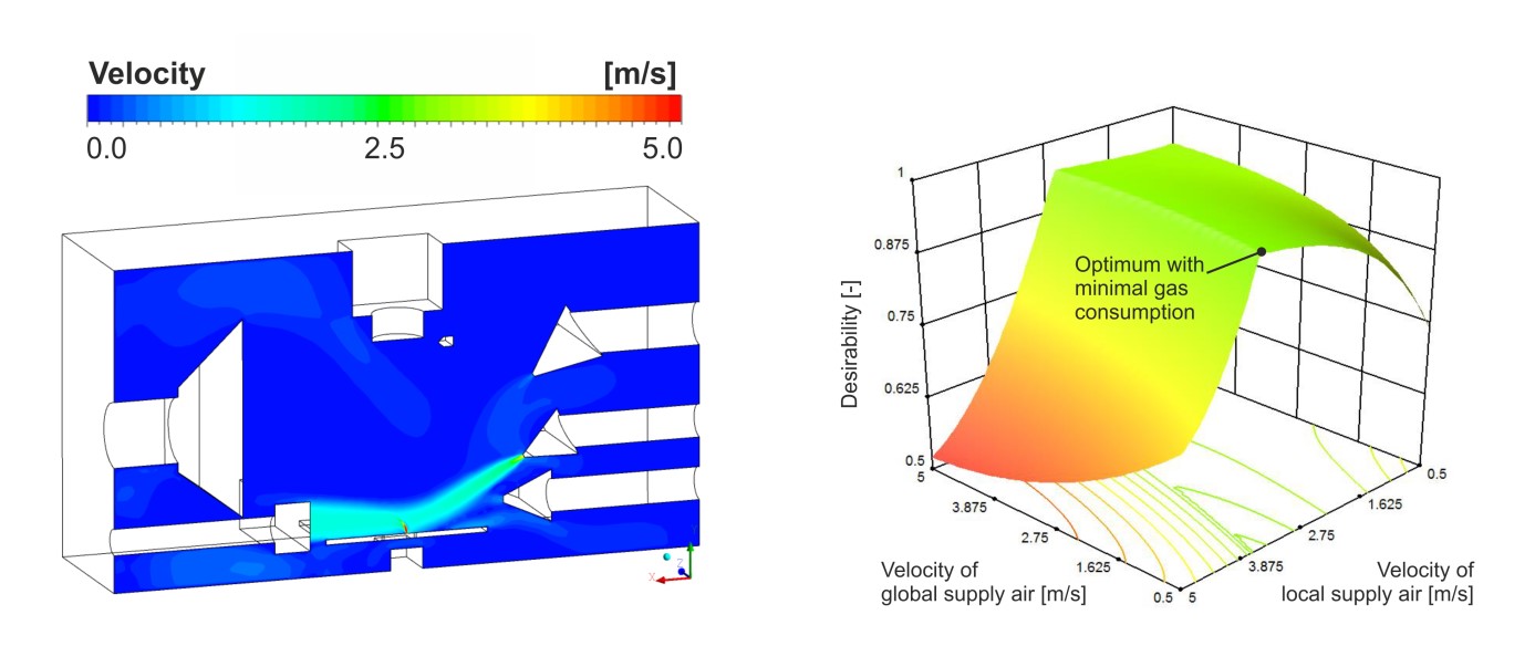
The experimental work was focused on the characterization of process phenomena and the determination of reliable welding conditions. For that purpose, a particular processing chamber was designed as shown in Figure 01. The interior view of this chamber shows inlet nozzles from a flat-jet type at different positions (1-3) on the right-hand side, as well as a global and a local exhaust air funnel (4-5) on the left-hand side. An additional cross-jet was applied to protect the laser optics (6). In this processing chamber, welding trials with a multi-mode fiber laser at an applied laser power of 3 kW and a welding speed of 2 m/min were performed on mild steel sheets with a thickness of 10 mm. Welds generated without any air flow showed no clear indications of a deep penetration process, and the weld depth was rather low. In contrast, the penetration was more than doubled under the influence of a well-defined gas flow. These findings emphasize the importance of an adapted cabin air flow with respect to the process efficiency. In the case of the investigations performed, local gas flow velocities in the range of 1 – 2 m/s above the weld zone were found to be sufficient to achieve this effect, and it was proven that larger values do not increase the penetration depth further on. In addition, it was found that a particular height of the welding plume is acceptable for stable welding regimes with maximum weld penetration depth. These processing conditions have been considered as a basis for optimization efforts regarding the cabin air flow.
However, with respect to the whole cabin flow, simple rules for an appropriate design are hardly available and optimal parameter configurations are difficult to find by means of empirical approaches because of the high number of control factors and factor combinations. To give an example, the individual air flow out of the applied flat-jet nozzle type is determined by 4 factors, namely the flow rate, the nozzle inclination, the distance to the processing zone and the outflow aperture. For the whole cabin air flow, 19 factors of influence have to be taken into account in total, which means that 219, i.e. more than a half million, factor-level combinations are possible if each factor is tested at only two value levels. Obviously, there is no alternative to Design-of-Experiments (DoE) methods which provide so-called screening designs to identify the most vital factors from a group of 19 factors with a minimal number of 192 runs. Such an analysis was performed by means of a Computational-Fluid-Dynamics (CFD) model to derive detailed information on cause-effect relationships regarding the cabin air flow. Exemplarily, Figure 02 (left) shows a computed air flow field for a particular parameter constellation. Process emissions were modeled as metal vapor inflow rate, and the height of a particular vapor concentration isoline was used as model response for the cabin flow evaluation. As a result of the screening analysis, 6 factors out of 19 were found as the most vital ones. With such a reduced number of factors, it became possible to apply a so-called multi-level Response-Surface-Method (RSM) as a basis for an air flow optimization. With a numerical effort of 157 additional computation runs, the functional dependencies between control factors and outcomes were quantified and described by a cubic regression model. Such a regression model is numerically easy to use and can be applied efficiently to determine optimal parameter configurations by computing the desirability function, plotted in Figure 02 (right) as a measure of the degree of fulfillment of defined optimization criteria, i.e. the limitation of the welding plume height to an acceptable level with minimal overall air or gas consumption.
The study has demonstrated a methodology to optimize the complex cabin air flow under the conditions of remote laser beam welding. However, the specific results cannot be generalized in a simple way as adaptable rules for the design of industrial processing cabins, because the characteristics of particular chambers, the spatial and temporal processing conditions, the type of applied air-flow components and the peculiarities of the specific welding applications always have to be taken into account for a profound analysis.
Acknowledgements
The work was performed in close collaboration by the Laser Zentrum Hannover e.V. (LZH) and the Fraunhofer IWS Dresden as part of the publicly funded research project “Steigerung von Prozessstabilität und Schweißnahtqualität beim Remote-Laserschweißen durch gezielte Strömungsführung mittels Anlagenadaption” (RemoStAad) with the reference number IGF 18149 BG. The authors acknowledge the financial and administrative support by the Bundesministerium für Wirtschaft und Energie (BMWi), the Arbeitsgemeinschaft industrieller Forschungsvereinigungen “Otto von Guericke e.V.” (AiF), the Forschungskuratorium Maschinenbau e.V. (FKM), and the Forschungsvereinigung Schweißen und verwandte Verfahren e.V. (DVS).
Figure 01: Interior view of the processing chamber with installed components (left) and weld seam cross-sections without (right a) and with air flow control (right b).
Figure 02: Computed air flow field (left) and desirability plot revealing parameter constellations for an optimized cabin flow (right).
By: Elena Lopez1, Tomás Felgueiras1, Christian Grunert1, Frank Brückner1, Mirko Riede1, André Seidel1,2, Axel Marquardt2, Christoph Leyens1,2, Eckhard Beyer1,2
1 Fraunhofer Institute for Material and Beam Technology, Winterbergstraße 28, 01277 Dresden, Germany
2Dresden University of Technology, 01062 Dresden, Germany
Introduction
Qualification and certification of parts made by AM processes has been identified by various authors [1, 2, 3, 4, 5] as one of the main challenges for the widespread adoption of AM in fabrication of structurally critical components. Traditionally, the qualification of parts is made by extensive non-destructive and destructive tests in a representative sample amount of the final product. This is a slow and expensive process in any kind of production, but in AM processes, it also contradicts many of the identified advantages, i. e. potential to save material and therefore process costs. To solve this problem, the qualification of AM parts demands a different approach, with focus in the research of certification of AM parts based on design and correlations of parameters during manufacturing and non-destructive tests [1, 4, 5]. This is attained through standards that are emerging to control key process factors and ensure uniformity and consistency across multiple machines and manufacturers. These standards are quite recent and started being published in 2013, with new actualizations appearing every year, in an effort of ASTM and ISO organizations to keep up with the fast paced development of AM technologies [1, 4, 5]. However, indirect methods such as build planning and process monitoring need further development to be broadly applied as a certification tool, which, for the time being, leaves final part qualification as the only way to warrant quality.
Due to the unique capability of AM technologies of making parts with complex geometrical forms and internal features, it is necessary to employ inspection methods that are capable of assessing part quality as a whole. Therefore, non-contact methods are the most promising tools to analyze AM parts, X-ray computer tomography (CT) and 3D scanning being the most prominent ones.
Within this paper the use of computer tomography for quality control of final parts was explored, with the geometrical complex demonstrator developed by Fraunhofer IWS as a test part. First, CT was used to explore process limitations of electron beam melting (EBM) to produce geometrically accurate parts. Second, different demonstrators made by selective laser melting (SLM) with different materials were also compared in terms of geometrical accuracy and finally, comparison of the CT with 3D scanning measurements were carried out and analyzed for the different demonstrators.
Experimental: Inspection techniques
X-ray computer tomography (CT)
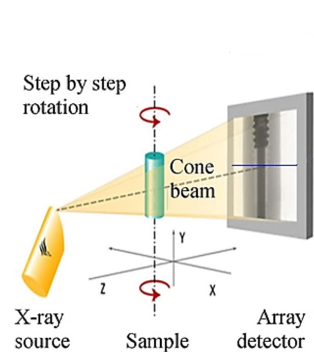
X-ray computer tomography (CT) uses electrically generated high intensity X-rays that pass through the investigated object from different angles as schematic represented in Figure 1. As X-rays pass through the object, they are attenuated due to absorption or scattering, generating different grey values. The total attenuation depends on the material composition, density and object thickness. The remaining X-ray fraction is registered by the detector generating hundreds or thousands of cross-sectional projections which are stacked together. Through mathematical algorithms, 3D voxels are created (3D pixel analog, with the associated grey value) which form the 3D reconstruction of the object.
Figure 1 – Computer tomography working principle
CT enables the scanning of all surfaces of an object, even if they are inside a part (e.g. cooling channels) because of the nature of X-ray. This results in a fully digitized object that allows a qualitative and quantitative characterization of the investigated object, giving exact information about the total part volume and wall thickness as well as porosities, cracks and inclusions [6].
The set-up used for the experimental work in this paper was a YXLON FF35 CT equipped with a 250 kV reflection X-ray vacuum tube with minimum spot size of ≤6 µm. In terms of detection, a 1792×2176 pixel YXLON flat panel 2530 detector was used.
3D Scanning
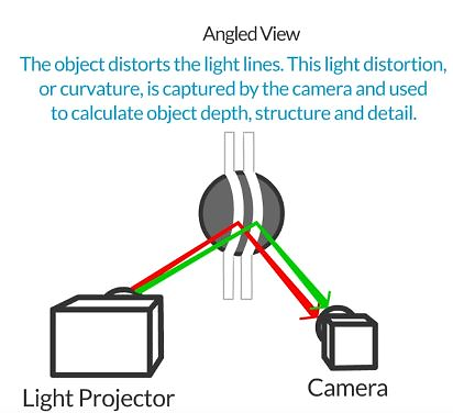
3D scanning uses structured light, i.e. a laser, that is projected on to the object which will distort the light direction depending on its shape. The light is captured by the camera and through triangulation the location of the measured point is calculated (see Figure 2). These points are afterwards processed by an algorithm and a 3D rendering of the object is made [7, 8].
Figure 2 – Working mechanism of structured light 3D scanner devices.
In the work presented in this paper, a GOM ATOS Core 45 was used (Figure 3) based in stereo fringe projection. In addition, it employs two cameras and a projector, that allows the capture of the object’s full surface geometry through a dense point cloud or polygon mesh[9].
Figure 3 – 3D scanner: GOM ATOS Core 45.
Demonstrators
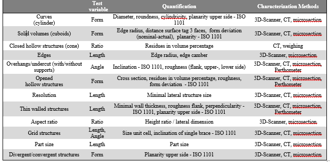
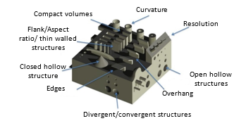
The use of demonstrators with defined complex geometrical features provide a proper way to evaluate the performance and benchmark of different AM techniques in order to determine process and geometrical accuracy, process repeatability and surface finish. The demonstrators in this paper are designed with challenging geometrical features with different sizes, like overhangs and thin wall structures. Different authors [10, 11, 12] proposed many different demonstrator designs, but some challenging geometrical features like internal channels have not been considered so far. The considered geometrical features at Fraunhofer IWS are detailed in Figure 4 and Figure 5 (see also Table 1). The demonstrator was also designed in a way that a scaling-up will ensure the comparison for Laser Metal Deposition.
Table 1 – Geometrical features extracted from the demonstrator and their quantification with suitable test methods.
Figure 4 – Defined demonstrator to evaluate different challenging geometrical features (see description).
Experimental Results and Discussion
Demonstrator Analysis
Several demonstrators made by different AM techniques were analyzed, as shown in Table 2. The analysis was made through X-ray computer tomography equipment YXLON FF35 CT, with the reconstruction software YXLON Reconspooler version 1.2.1.0 and the software VGStudio MAX 3.0 for the nominal/actual comparison and porosity analysis.
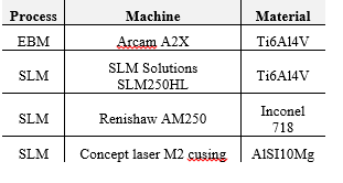
Table 2- Processes, machines and materials used for the building up of demonstrators.
EBM Demonstrators
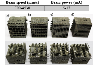
On the analysis of the EBM parts, four demonstrators were considered. They were built with the same parameters (Table 3) but different support base square grid sizes as shown in Figure 5).
Table 3 – Build parameters of the EBM demonstrators.
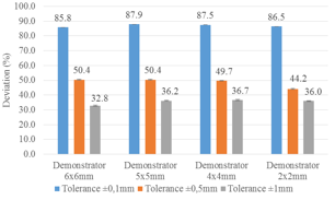
Figure 5 – EBM Ti6Al4V demonstrators with different square base sizes: a) 6x6mm square size; b) 5x5mm square size; c) 4x4mm square size; d) 3x3mm square size.
The EBM demonstrators did not accurately reproduce the features proposed originally, since they suffered from swelling on the Z direction, distorting the overall part (Figure 6). This defect indicates that high beam energies of 300 J/m and above were used [13]. Adding to the swelling in the Z direction the demonstrator also suffered from retraction around the part and the excessive building temperature led to sintering of powder inside the internal channels.
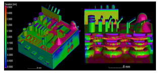
Figure 6 – Left: EBM demonstrator 6x6mm comparison at ±0,5mm deviation with the CAD file. Right: Perpendicular cut of the EBM demonstrator 6x6mm with comparison at ±0,5mm deviation with the CAD file, where the deviation of the channels can be observed
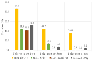
Comparison of deviation percentage of EBM demonstrators at different tolerance distances (Figure 7) revealed a positive effect of smaller square grid size, promoting higher heat transfer part/base, resulting in less distortion. However, even at ±1 mm deviation the demonstrators didn’t reach an ideal minimum threshold of 10% deviation. The 6x6mm demonstrator displayed the highest distortion visually, though displaying slightly best results at ±0.1 mm and ±1 mm tolerance (85.8 and 32.8%). This effect might be due to the automatic registration of the part made on VGstudio MAX which will tend to decrease the deviation between part and CAD file achieving a best fit.
Figure 7 – Deviation of EBM demonstrators at different tolerances.
SLM demonstrators
Three different materials have been chosen for the manufacturing of the SLM demonstrators (Ti6Al4V, Inconel 718 and AlSi10Mg). These materials have been selected due to their relevance for the manufacturing of parts for the aerospace, space and energy sectors. The influence of the material selection on the dimensional accuracy will be also analyzed and discussed in this paper (Figure 8).
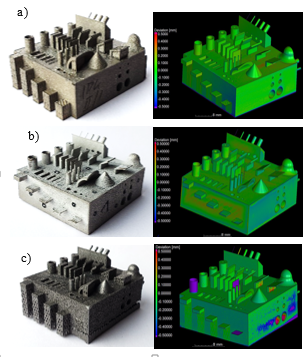
Figure 8 – SLM demonstrators as built and respective comparison with CAD file (right) at ±0,5mm. a) Ti6Al4V; b) Inconel 718; c) AlSi10Mg.
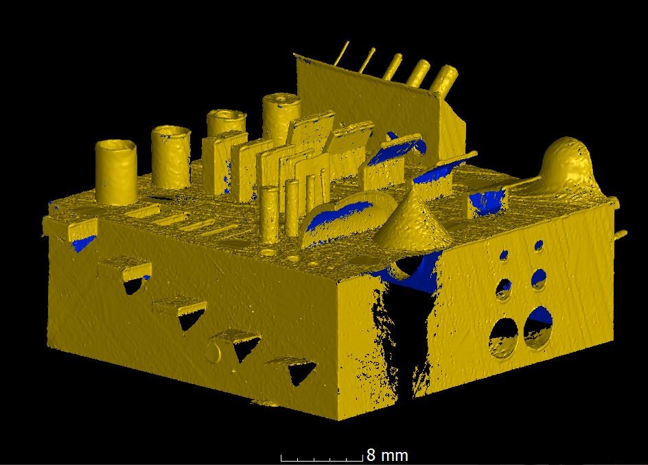
The analysis of the comparison for the SLM demonstrators pointed out that the material composition of the part affects the minimum feature possible, since the only appropriate demonstrator in order to reproduce all geometrical details was the one built up with Inconel 718, most probable because of the higher melting temperature of Inconel, allowing better metal melt pool control. The Ti6Al4V SLM demonstrator showed low deviation values even though it was not feasible to reproduce the columns with dimensions 0,1mm thin wall structures while also suffering from warpage and even detaching from the support structure (Figure 9).
Figure 9 – Detail of the AlSi10Mg demonstrator.
Overall analysis on Figure 10 confirms the superior capability to reproduce fine details and better geometrical accuracy by SLM compared to EBM. However, the production of parts with tolerance inferior to ±0.5 mm appears to be the limit of SLM, being dependent on material choice for detailed feature reproduction.
Figure 10 – Deviation comparison between the demonstrators made by different techniques.
The porosity analysis of the SLM Ti6Al4V demonstrator has been carried out revealing a residual porosity of 0.018% (Figure 11). The cause of this porosity was an obstruction of the 0.5 mm internal channels with residual powder.
Figure 11 – Porosity analysis of the SLM Ti6Al4V demonstrator.
Comparison of Computer Tomography against 3D scanning
The use of the 3D scanning generated insufficient results (Figure 12) since a firm attachment mechanism to the base was needed to prevent movement of the part during the capture of the features from more angles, which otherwise would diminish the precision. This led the structures to create shadows and the high reflectivity of the metal part hindered the surface recognition. This generated a partial representation of the demonstrator, rendering it unfit for total comparison with the original CAD file.
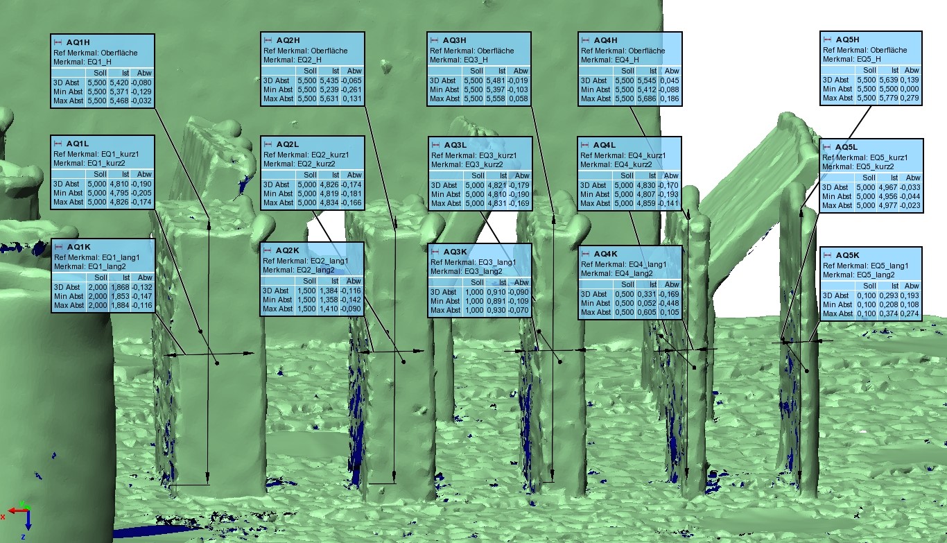
Figure 12 – Stl file obtained by the GOM Atos 45 with 0.4 mm dot size of the SLM Inconel 718 demonstrator.
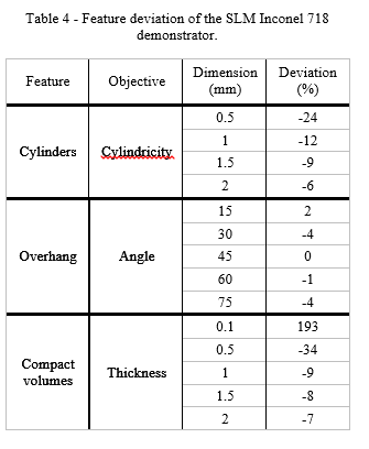
However, with the determined surface it was possible to make a analysis of the deviation of the features (Figure 13) using the software IMInspect 2015 IR4 by Innovmetric Software Inc. The results on Table 4 show higher deviations for lower dimension features, by which the machine was not capable of reproducing the 0.2 mm cylinder. These results corroborate the total comparison by computer tomography of minimum feature capability of features <0.5 mm.
Figure 13 – Feature deviation measurement of the Stl. SLM Inconel 718 demonstrator obtained by the GOM Atos 45.
Table 4 – Feature deviation of the SLM Inconel 718 demonstrator.
On the other hand, the CT measurements were capable of fully characterizing the demonstrators, being able to display internal features, like the internal channels and the corresponding typical defects on overhang structures, that would be impossible to carry out by other methods.
Conclusions
Optical methods are insufficient for final part qualification due to their incapability to analyze internal features and the reflectivity of the surfaces of some parts that hinders accurate measurements. 3D scanning might be good for surface feature measurement, but it is insufficient for full characterization of an AM demonstrator of the addressed complexity aiming to explore the geometrical limits of additive manufacturing.
On the other hand, computer tomography can quantify all complex structures in scope of the proposed demonstrator and delivered deviation values of the measured structured, providing a good base for comparison across demonstrators made by different methods, materials and dimensions. Porosity or defects down to 3 µm can be determined by the used CT system.
The overall analysis confirmed the superior capability of SLM compared to EBM to reproduce fine details and better geometrical accuracy. However, the production of parts with tolerance inferior to ±0,5mm appears to be the limit of SLM, being dependent on material choice for detailed feature reproduction.
The subsequent comparison by means of computer tomography of the proposed demonstrators and the process conditions, allows one to deduce the most appropriate process parameters within a relatively small amount of experiments.
CT is the inspection and validation method of final parts that best fits the necessities of the AM industry. However, it is still a time-consuming procedure that requires several hours to set, run and analyze measurements and generate a report for each new part, which is not desired on an industrial environment. With the expected expansion of the AM market, CT machines development requires more focus on the necessities of the AM industry in order to shorten scanning and analysis time and turn CT measurements into an online quality control method of final parts in the manufacturing process.
References
[1]W. E. Frazier, “Metal additive manufacturing: A review,” J. Mater. Eng. Perform., vol. 23, no. 6, pp. 1917–1928, 2014.
[2]I. Gibson, D. Rosen, and B. Stucker, Additive Manufacturing Technologies. New York, NY: Springer New York, 2015.
[3]S. L. N. Ford, “Additive Manufacturing Technology : Potential Implications for U . S . Manufacturing Competitiveness,” J. Int. Commer. Econ., vol. 6, no. September, pp. 1–35, 2014.
[4]I. Wing, R. Groham, and B. Sniderman, “3D opportunity for quality assurance and parts qualification: Additive Manufacturing clears the bar,” Deloitte Univ. Press, 2015.
[5]Y. Huang, M. C. Leu, J. Mazumder, and A. Donmez, “Additive Manufacturing: Current State, Future Potential, Gaps and Needs, and Recommendations,” J. Manuf. Sci. Eng., vol. 137, no. 1, p. 14001, 2015.
[6]L. De Chiffre, S. Carmignato, J. P. Kruth, R. Schmitt, and A. Weckenmann, “Industrial applications of computed tomography,” CIRP Ann. – Manuf. Technol., vol. 63, no. 2, pp. 655–677, 2014.
[7]F. Chen, “Overview of three-dimensional shape measurement using optical methods,” 2017.
[8]C. Xiaobo, X. Jun, J. Tao, and J. Ye, “Research and development of an accurate 3D shape measurement system based on fringe projection : Model analysis and performance evaluation,” vol. 32, pp. 215–221, 2008.
[9]P. Kühmstedt, C. Munckelt, M. Heinze, and C. Bräuer-burchardt, “3D shape measurement with phase correlation based fringe projection,” Opt. Meas. Syst. Ind. Insp., vol. 6616, pp. 1–9, 2007.
[10]P. Shah, R. Racasan, and P. Bills, “Comparison of Different Additive Manufacturing Methods Using Optimized Computed Tomography,” 6th Conf. Ind. Comput. Tomogr., vol. 1, pp. 1–10, 2016.
[11]S. Moylan, J. Slotwinski, A. Cooke, K. Jurrens, and M. A. Donmez, “An Additive Manufacturing Test Artifact,” vol. 119, pp. 429–459, 2014.
[12]A. Thompson, I. Maskery, and R. K. Leach, “X-ray computed tomography for additive manufacturing: a review,” Meas. Sci. Technol., vol. 27, no. 7, p. 72001, 2016.
[13]A. Kirchner, B. Kloden, J. Luft, T. Weisgarber, and B. Kieback, “Process Window for Electron Beam Melting of Ti-6Al-4V,” Euro PM2014 – AMTechnologies, pp. 6–11, 2014.
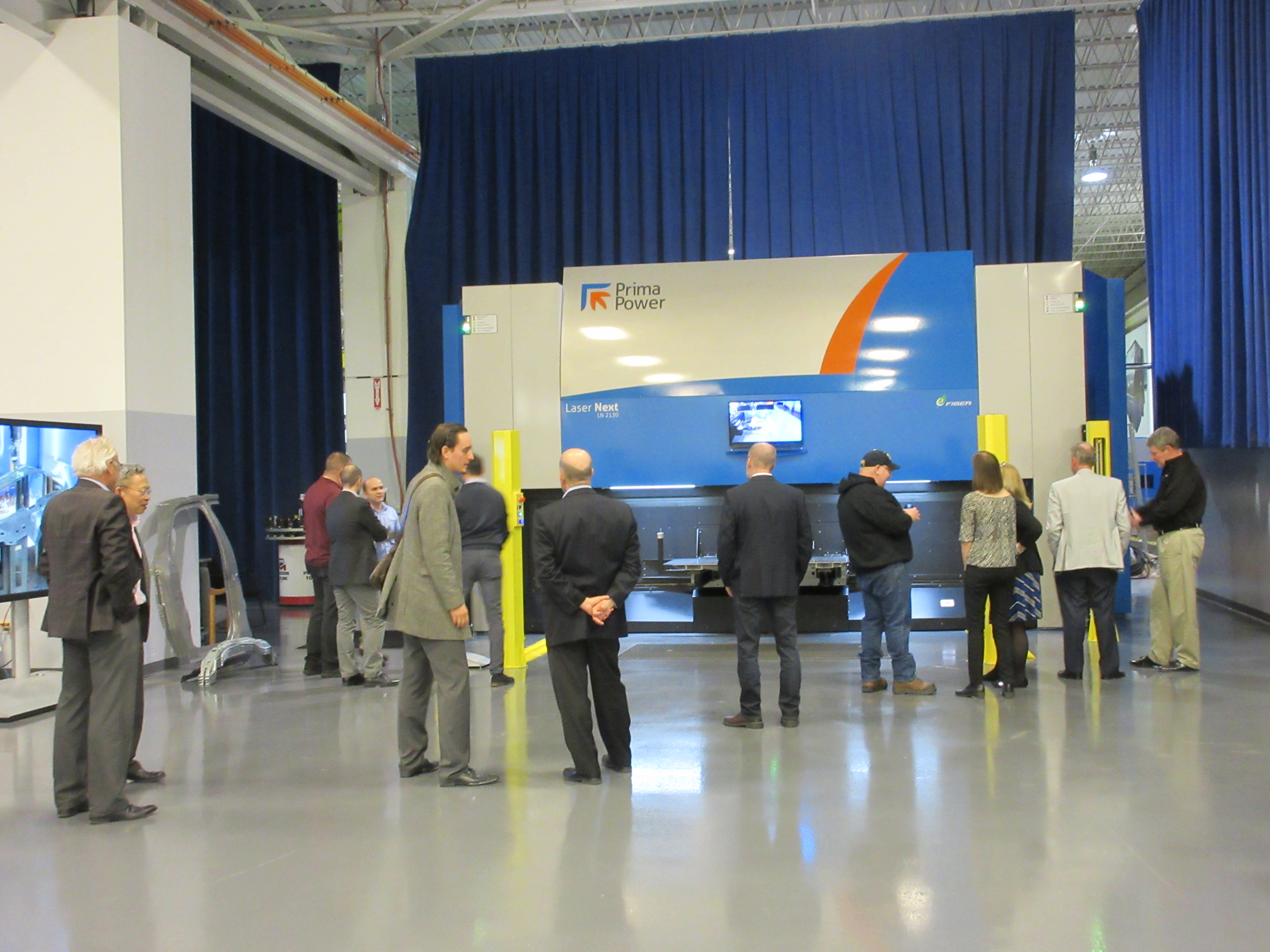
Prima Power was an exhibitor at Laser Institute of America’s LME 2018, held March 28-29 at the Renaissance Schaumburg Convention Center, Schaumburg, IL. After show hours on March 28, Prima Power hosted an Open House at its showroom in nearby Arlington Heights, IL. A large group of visitors, composed of laser industry experts, suppliers, and prospective customers were able to get a close-up view of the Prima Power Laser Next 3D Laser.
Thanks to a deep and unique experience of over 35 years in this field and to a continuous dialogue with customers and partners operating in the car industry, Prima Power has designed the new 3D laser machine for automotive production: Laser Next. In developing Laser Next, Prima Power has focused on the achievement of the following main benefits for the user:
Maximizing throughput with a dramatic reduction of cycle times. During the last 10 years, the performance of Prima Power 3D laser machines for automotive applications has been growing steadily. With Laser Next, a fundamental step forward was made: productivity on a typical benchmark component (B-pillar) was raised by 25%. In other words, four Laser Next systems produce as much as five machines of the previous model.
Space-efficient layout both for stand-alone and multi-machine configuration. Space is money, and a well-conceived layout helps save square meters and optimizes plant logistics. The compactness of the installation further improves installing more machines, since you can have up to three units one next to the other connected to the same magnetic scrap conveyor, with no need of excavation works. Given the same area, in fact, it is possible to install more machines (e.g. four Laser Next instead of three units of the previous model). Considering the performance of Laser Next, the productivity per square meter ratio is simply astonishing.
Improved Overall Equipment Efficiency (OEE). For Laser Next, Prima Power capitalized on its experience of hundreds of installations for the 24/7 manufacturing of high-strength steel components, widely used in car production.
Every detail was studied and developed to maximize machine uptime. Maintenance was also lowered and simplified to reduce non-productive times and the need of specialized resources dedicated to these activities.
Laser Next has a working range of 3,050 x 1,530 x 612 mm and is equipped with 3 kW or 4 kW high brilliance fiber laser. Its compact focusing head, fully sealed for best protection, features direct drive motors, double protection SIPS, fully-metallic sensor, and Focal Position Control.