Superhydrophobic and Superhydrophilic Functionalization of Engineering Surfaces by Laser Texturing

By Suwas Nikumb, Peter Serles, and Evgueni Bordatchev

As seen in ICALEO 2017 and LIA TODAY


Nature is a bountiful source of inspiration to advance innovative surface functionalities, processes, and technologies for engineering materials. For example, the super-hydrophobic surface characteristic of the lotus leaf can be recreated by mimicking the microstructure and surface energy on stainless steels. This super-hydrophobic behavior, which causes water to roll off the lotus leaf while collecting dust particles, enables the self-cleaning of the leaf surface and is primarily due to the hierarchical conical structures, as well as the wax layer present on the leaf surface. A good understanding of the surface topography of the microstructures, water droplet contact angle, and surface chemical composition provides the important clues necessary for the creation of artificial super-hydrophobic or superhydrophilic surfaces and using state-of-the-art ultrafast laser ablation treatment.
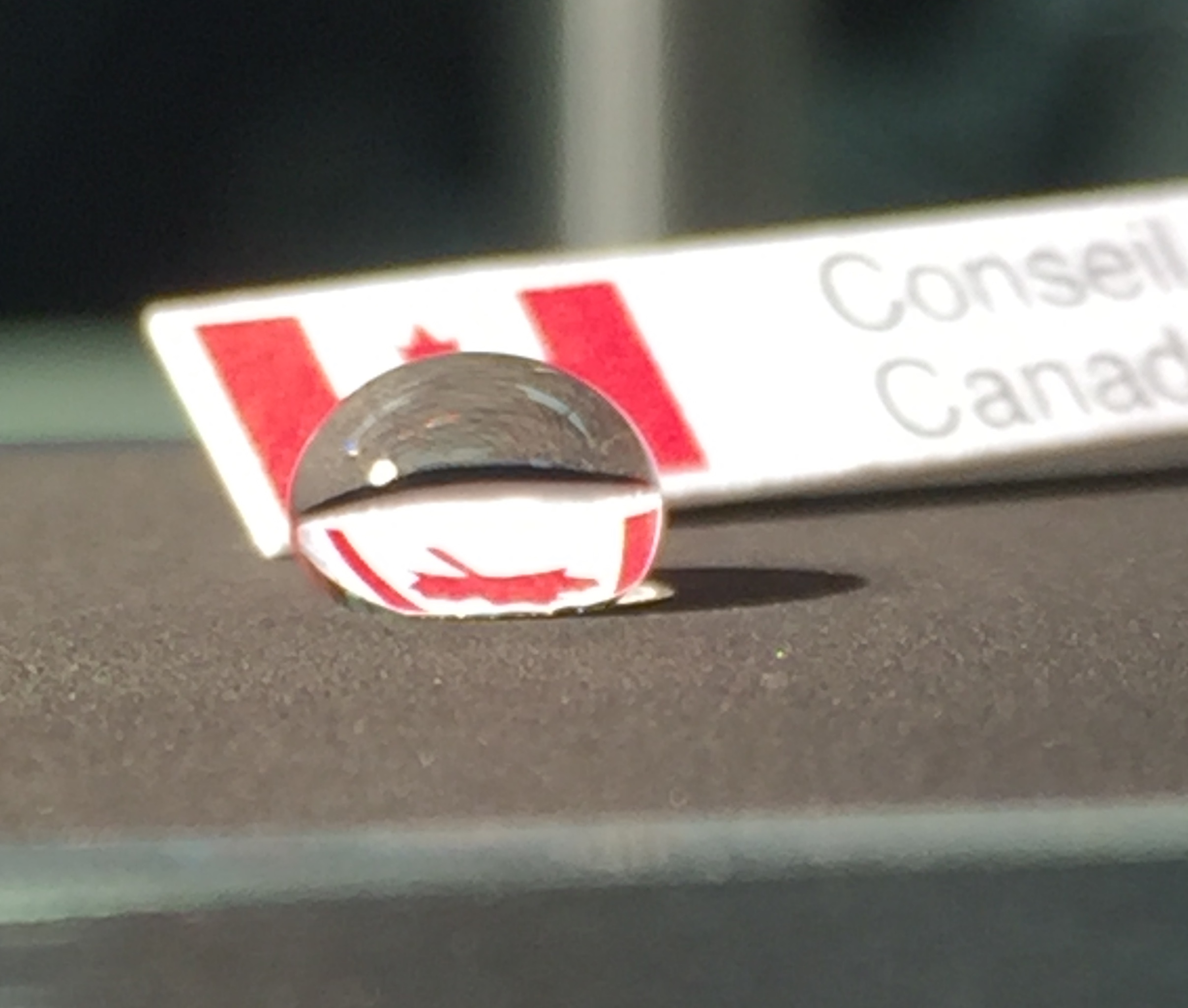
Figure 1

Controlling the wettability of a material surface for superhydrophobic or superhydrophilic performance has been an interesting area where numerous different methods are being pursued. While many coatings and thin-films are able to achieve extremely high or low wettability, their endurance life, chemical compatibility, and large area scalability make them less attractive for manufacturing environments. Meanwhile, ultrafast pulsed lasers with several megahertz pulse repetition rates can tune the wettability of a surface without changing its chemical composition and offers higher endurance lives. This is accomplished by instant vaporization (laser ablation) of the material in specific micro-scale patterns thus creating structures that changes the way the surface topography interacts with water.

A superhydrophobic surface is characterized by its ability to repel water using structures that are akin to a bed of nails allowing the water droplet to rest only on the peaks using surface tension and therefore repel from the surface (see Fig.1). Contrarily, a superhydrophilic surface is characterized by its ability to attract and spread the water so features a series of channels that trap water and wick it away using micro-capillary forces. Such surface functionalization techniques have been developed at Canada’s National Research Council for stainless steel (304 SS) and Silicon Carbide (SiC) surfaces respectively to demonstrate the effectiveness of laser texturing technology for wettability control of common engineering surfaces. Fig.2 depicts superhydrophobic performance of a bouncing water droplet at ~5° tilt on 3×3 cm2 textured area.

Experimentally, a 10 W picosecond pulsed laser operating at 1 MHz frequency was focused to a tiny spot of 25 µm diameter. The samples were mounted on a CNC motion system equipped with argon gas protective environment. The optimization of laser structuring process included varying each of the laser parameters, e.g. power, frequency, feed rate, grid pitch, etc. and evaluating the water droplet contact angle using the standard drop-shape analysis method. For the 304 SS superhydrophobic surface, a laser beam fluence of 2.61 J/cm2 was used to promote narrower, shallower features by material redistribution rather than complete vaporization, while the SiC superhydrophilic surface was realized using a much higher fluence of 10.7 J/cm2 to create thicker and deeper channels for the water to impregnate. Both surfaces were machined using the five-axis CNC micromachining system to texture grid patterns, ensuring an even distribution of micro-structures.
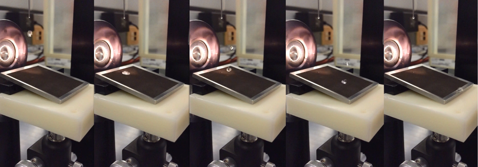
Figure 2


The superhydrophobicity of 304 SS surface was highly dependent on post-processing conditions in order to tune the wettability. Specifically, the chemical nature of the surface was reactive for 14 days after laser processing due to high-power interaction with the material which excites the chemical state. The samples were thus stored in different environments and exhibited vastly different contact angles. Most notably, the sample which was submerged in deionized water showed hydrophilic tendencies while the sample kept in extremely dry (<8% relative humidity) air was highly superhydrophobic with a contact angle of 152º. Following this two week period, the sample attained stable chemical equilibrium and the wettability was unchanged regardless of environment.
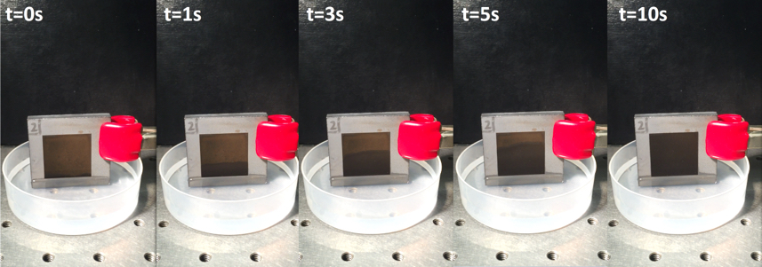
Figure 3

The superhydrophilic SiC surface on the other hand was not as reactive and therefore showed a contact angle of 0º immediately after processing. As aforementioned this sample was intended to have wider and deeper channels to hold and wick the water away from the contact point. The micro-capillary forces that are responsible for spreading the water across the surface were strong enough even to counter gravity; Figure 3 shown below depicts a time-lapse of a 3×3 cm2 textured area placed vertically with the bottom edge in water. Within a 10-second span, the entire surface was wet by the micro-capillary forces pulling water vertically against the force of gravity.

The potential for laser texturing technologies spans many applications in manufacturing industries. Superhydrophobic surfaces have been proposed as a method to mitigate many fluid problems; by decreasing the interaction between a pipe wall and the fluid, the drag experienced by the fluid has been shown to decrease significantly in both laminar and turbulent flows. Thus far, only superhydrophobic coatings and thin-films have been tested for this application however they remain plagued by rapid wear and very short lifetimes. The robustness of the laser texturing process to achieve superhydrophobicity therefore presents exciting new opportunities. As well as water repellency of superhydrophobic surfaces, longer freezing times of water droplets and lower adhesion strength of ice to the surface are characteristics of these high contact angle surfaces and thus present an iceophobic surface property. This enables applications for machinery that operate in colder climates such as wind turbines and airplane wings and engines.

Applications for superhydrophilic surfaces are commonly based on the micro-capillary forces demonstrated as the rapid dispersion creates a thin film of water on the surface. This thin film allows for an increased rate of evaporation from the surface opening doors for anti-fogging applications or greatly increased rates of heat transfer. Other applications manipulate the thickness of the film formed which can provide antireflection ability for surfaces such as solar cells. Superhydrophilic textured surfaces also exhibit increased adhesion strength with the liquid due to the impregnation of the liquid into the surface, therefore providing applications for improvement in bonding strength of joints between different material surfaces.

The wettability control functionalization on engineering surfaces opens the door for new applications with both superhydrophobic and superhydrophilic surfaces. The robust nature of laser surface texturing technologies in combination with chemical compatibility and industrial scalability makes this method unique and most promising to deploy a wide range of functions in manufacturing products. While this technology has already provided solutions to several significant industrial tasks, many more applications are currently being explored at NRC.


More details on this topic can be found on YouTube: Combined Wettability Control (https://youtu.be/7IW2aC_rkjw), Super-hydrophobic Bouncing (https://youtu.be/b1vXDuvf3aQ), Super-hydrophilic Ceramic (https://youtu.be/9ZCcW4cOccw), along with other presentations on NRC’s micro/nano-machining capabilities. Further details on these studies can be found in: Superhydrophobic and superhydrophilic functionalized surfaces by picosecond laser texturing. Journal of Laser Applications 30, 032505 (2018); https://doi.org/10.2351/1.5040641

Laser direct writing: An effective approach to flexible hybrid electronics

As featured in the LIA TODAY and ICALEO 2017

By Jinguang Cai and Akira Watanabe

The development of miniaturized portable and wearable electronic devices has attracted worldwide research attention, due to their increasing integration with human daily life. Different from traditional electronic devices on “hard” boards, such devices should be soft and flexible. A concept called “flexible hybrid electronics”, which is a hybrid of soft and hard parts, has been proposed to address the fabrication issue of flexible devices.

Fig. 1. A schematic image of a simple flexible hybrid electronic device.

The concept of a flexible hybrid electronic device is illustrated in Fig.1, in which “soft parts”, such as electronic interconnection, energy harvesting and energy storage components, antennae, and even displays, sensors, and communication interfaces, can be prepared via printing methods. “hard parts”, such as processor and memory, can be provided by the commercial small-size silicon components, which are small enough, and can be integrated into the device without influencing the flexibility. However, printing methods have some issues such as limitation of materials, high cost of inks, and complicated post-processing.

Laser direct writing is a non-contact, fast single-step fabrication technique without requirements for masks, post-processing, and complex clean environments. Meanwhile, various kinds of lasers have been rapidly developed with relatively low costs and broad available wavelengths and powers, and widely used in industry for materials welding, cutting, and polishing. Besides, laser processing can be focused into a micrometer-sized or submicrometer-sized area to realize on-demand fabrication of functional micro-patterns, showing the potential to be integrated into current product lines for commercial use. Laser direct writing has been demonstrated to prepare energy harvesting and energy storage components, electronic circuits, sensors, communication interface, and antennae.

Energy harvesting and storage components

Generally, a flexible device employs a thin film battery as the energy storage and supply unit, in combination with a flexible energy harvesting device such as a polymer solar cell. Recently, as a new type of energy storage device, micro-supercapacitors (MSCs), has been developed and recognized as potential power supply units for on-chip micro-devices, because they possess not only the advantages of supercapacitors such as high power density, excellent cycling stability, pollution-free operation, maintenance-free feature, and flexibility, but also simplified packaging processes and compatibility with integrated circuits. Among various materials for supercapacitors, carbon materials possess the properties which can satisfy the requirements of MSCs in the flexible devices, such as high specific surface area, high electrical conductivity, high electrochemical stability, and high mechanical tolerance.

Fig. 2. A carbon micro-supercapacitor prepared by laser direct writing.

Laser-induced carbonization of polymers such as polyimide has been demonstrated to prepare flexible all-solid-state carbon-based MSCs with high performance by laser direct writing on a polyimide (PI) film in air (Fig. 2). In order to suppress the oxidation process and thus, increase the conductivity of the laser-induced carbon structures, the laser direct writing was conducted on PI films in an inert gas such as Ar, resulting in carbon MSCs with improved volumetric energy density and power density. Furthermore, high-conductive Au nanoparticles can be incorporated to construct double-layer carbon/Au composite electrodes with improved conductivity by two-step laser direct writing.

It will be beneficial for practical use if energy harvest and storage units can be integrated into the same device. As a demonstration, TiO2 nanoparticles were deposited on one side of the laser-written interdigitated carbon electrodes by an electrophoretic method, forming carbon/TiO2 composite MSC with photo-rechargeable capability under UV irradiation due to the photovoltaic property of TiO2 nanoparticles. Although the charging voltage is not high enough for practical use currently, it is expected that such a strategy can be developed for practical use by optimizing the photo-absorption materials and the combination.


Fig. 3. Schematic images of an integrated photodetector (top) and a rGO/GO/rGO humidity sensor (bottom) prepared by laser direct writing.


Photodetectors and humidity sensors

Sensors are one of the most important interfaces with users in IoT (Internet of Things) technology, thence it is very important to develop various types of sensors for flexible devices. Laser direct writing can play an important role in preparing sensors directly on the flexible substrate with high performance and stability. For example, a photodetector for UV light can be fabricated by laser direct writing and deposition of ZnO nanoparticles, and can be integrated into the PI film with a carbon MSC fabricated by laser-induced carbonization, forming an integrated photodetector for practical use (Fig. 3, Top). Besides, a humidity sensor based on an interdigitated reduced graphene oxide (rGO)/graphene oxide (GO)/rGO structure prepared by laser direct writing was also demonstrated with high and fast response, flexibility, and long-term stability, showing the potential to be used in flexible devices (Fig. 3, Bottom).

Fig. 4. Schematic images of an integrated wireless charging and storage device (top) and an NFC tag (bottom) prepared by laser direct writing in combination with electroless Ni plating.

Circuits, communication interface, and antenna

High-conductive metallic circuits with mechanical stability are very important in flexible devices as basic structures, and their preparation should be facile, cost-effective, and easily integrated with other electronic components. Laser direct writing has been demonstrated to pattern metallic Pd on PI films, which can act as catalysts in the electroless Ni plating process, producing high-conductive carbon/Ni composite structures. The carbon/Ni structures exhibited a certain flexibility and excellent anti-scratch performance due to the intimate deposition of Ni layer on carbon surfaces. Such carbon/Ni structures can be used as conductive circuits to construct practical devices.  For example, a wireless charging and storage device can be fabricated by integrating an outer rectangle carbon/Ni composite coil for harvesting electromagnetic waves and an inner carbon MSC for energy storage, which can be fast charged by a commercial wireless charger (Fig. 4, Top). In addition, a near-field communication (NFC) antenna was prepared using a carbon/Ni composite coil, and acted as a communication interface with an NFC smartphone for harvesting signals, and an ultra-small commercial IC chip was integrated for data storage (Fig. 4, Bottom). The integrated NFC tag can be used for practical application.

Summary & outlook

While laser direct writing has been demonstrated to be an effective approach to preparing most of the components in flexible devices, such as carbon MSCs as energy storage unit, carbon/TiO2 MSCs for energy harvesting and storage unit, photodetectors and humidity sensors, high-conductive carbon/Ni structures for electronic circuits, and even integrated wireless devices, many efforts are still required to promote the laser direct writing technique applied in the development of flexible hybrid electronics for practical applications in IoT in the future.


Jinguang Cai, Institute of Materials, China Academy of Engineering Physics, Jiangyou 621908, Sichuan, P. R. China

Akira Watanabe, Institute of Multidisciplinary Research for Advanced Materials, Tohoku University, 2-1-1 Katahira, Aoba-ku, Sendai 980-8577, Japan

Inventors Synthesize Graphene with Lasers

As featured in the LIA TODAY

By Liliana Caldero

Graphene – it’s the two-dimensional (2D) allotrope of carbon atoms that ignited the imaginations of researchers across the globe. Heralded as a ‘miracle material’, its potential seemed limitless and it was predicted to usher in the next generation of technology. Flexible, stronger than steel, transparent, lightweight, and an amazing conductor of heat and electricity, it was going to revolutionize everything from household electronics to biomedical nanotechnology.


THE PROBLEM

Yet, nearly eight years after Dr. Andre Geim and Dr. Konstantin Novoselov earned the Nobel Prize in Physics for first isolating graphene and identifying its properties, graphene has encountered barriers to moving out of the lab and into the marketplace. According to Prof. Dr. Aravinda Kar of the University of Central Florida’s Center for Research and Education in Optics and Lasers (CREOL), one of the most prominent barriers has been finding scalable manufacturing processes that can produce graphene of a quality and quantity ready for consumers and businesses.

Graphene is notoriously difficult to synthesize in large quantities at a consistent quality. Early methods of isolating graphene involved a slow and tedious mechanical exfoliation technique; the researchers would extract a thin layer of graphite from a graphite crystal using regular adhesive tape, continually reducing the graphite sample by sticking the tape together and pulling it apart until only a small, 2D section of carbon atoms with a honeycomb lattice remained. Graphene’s unique characteristics are only present when it is one, two, or three layers of atoms thick – any thicker and it becomes graphite, losing all of the exceptional properties of graphene. The tape exfoliation method, although useful for the lab, was not going to translate very well to an industrialized process.


SOLVENT-AIDED EXFOLIATION AND CVD

Two of the more promising and potentially scalable methods of producing graphene are solvent-aided exfoliation and chemical vapor deposition (CVD). In solvent-aided exfoliation, sonication is used to exfoliate graphene crystals which are then further separated in a solvent and later gathered into graphene monolayers.  Scientists at the National University of Singapore have identified a flocculation method that reduces the amount of solvent needed for their exfoliation process, which could yield graphene using far less solvent than was previously needed. Another method experiencing innovation is CVD, which uses thermal chemical reactions to ‘grow’ graphene on substrates of specific materials, typically copper or silicon. Recently, engineers at MIT developed a CVD process for producing graphene filtration membrane sheets at 5 cm per minute. One of the biggest issues with traditional CVD and exfoliation methods is the need to transfer graphene from its fabrication platform to a substrate. Lasers are going to change that.


THE MISSING PIECE – LASERS

Lasers may provide yet another avenue to the elusive mass production of graphene, with an eye toward innovating the semiconductor industry. In 2003, Kar, along with Dr. Islam Salama and Dr. Nathaniel Quick, realized that laser direct writing could be used to fabricate carbon-rich nanoribbons on a silicon carbide (SiC) wafer in a nitrogen rich environment. Although these ribbons were too thick to be considered graphene, Kar believed that with a few changes, this process could be reworked to synthesize graphene in situ on a large scale, very quickly. In 2013, Kar and Quick were issued a patent for a Laser Chemical Vapor Deposition (LCVD) method that could be scaled for mass production.

Their method involved a few simple components: a frequency doubled Nd:YAG (green) laser of 532 nm wavelength, methane (CH4) gas, a silicon substrate, and a vacuum chamber.

The 532 nm wavelength corresponds to a photon of energy 2.33 eV, so the energy of two photons is 4.66 eV, just within the range of the C-H bond energy (4.3-4.85 eV) in CH4. Focusing the laser beam to a high intensity can induce two-photon absorption at the focal plane, causing the decomposition of CH4 to release the hydrogen atoms and deposit carbon atoms only on the substrate. The laser heating of the silicon substrate is just low enough to avoid melting the silicon, while providing sufficient thermal and electromagnetic energies to assist the carbon-carbon bonds rearrange into graphene’s trademark hexagonal pattern.

An experimental set-up for multiphoton photolytic laser chemical vapor deposition (LCVD) of graphene from methane precursor. Image courtesy of Dr. Kar and Dr. Quick.

LASER DIRECT WRITING OF GRAPHENE

Kar believes this process could be adapted to add graphene directly onto any substrate. Using laser direct writing, a company could easily draw graphene circuits onto a board. For companies using a hybrid approach, the graphene could be deposited at precise points as interconnects. “You would have all the CAD/CAM capability you could want,” says Quick. Currently, green lasers are available at high output powers, 100 W in continuous wave mode from most large laser manufacturers, so adding this additional step to the manufacturing pipeline for semiconductors would be easy and inexpensive compared to other methods.

At 1.9 cm per second, or 45 inches per minute, this method of graphene production is fast and efficient. This LCVD method offers control over the number of graphene layers, whether one, two, or three are required.  This process also removes the need to manually place graphene onto its intended location, as it is synthesized precisely where it should be. It’s also worth mentioning that this process is conducive to minimal environmental impact, as the unreacted methane and hydrogen byproducts can be captured to be recycled and reused.


A LOOK AT THE FUTURE

Picture this: a template is placed over a substrate and a line-shaped laser beam sweeps over it briefly or a beam of large cross-sectional area illuminates the entire template in one shot; when the template is removed, an intricate graphene design has been printed onto a circuit board. That is the future that Kar says is possible, with the right equipment. He suggests that we need manufacturers to develop lasers producing line-shaped beams or large area beams with spatially uniform intensity profile to realize this vision cost-effectively. He emphasizes that a true line-shaped beam produced by a slab laser system or an array of optical fiber laser would be necessary, as shaping the beam synthetically by changing the shape of an aperture would result in too much lost energy. With this technology, graphene could easily be printed onto circuit boards immediately, only where it’s needed, saving in material costs and time.

Nearly 14 years after the excitement first began, researchers are still exploring the potential uses of graphene; from applications in microsupercapacitors to Organic LEDs in flexible displays to ultra-sensitive optical sensors, and even lightweight body armor, the possibilities are still as exciting as ever.


Acknowledgements

Prof. Dr. Aravinda Kar, University of Central Florida, CREOL

Dr. Nathaniel Quick, Executive Director of LIA


LEARN MORE

Laser Formation of Graphene: United States Patent 8617669. (N. Quick, A. Kar)
http://www.freepatentsonline.com/8617669.html

NUS-led research team develops cost effective technique for mass production of high-quality graphenehttp://news.nus.edu.sg/press-releases/mass-production-graphene-slurry

MIT researchers develop scalable manufacturing process for graphene sheetshttps://newatlas.com/mit-manufacturing-graphene-filtration-membranes/54274/

Design Guidelines For Laser Metal Deposition of Lightweight Structures

Design Guidelines for Laser Metal Deposition of Lightweight Structures

By Ake Ewald and Josef Schlattmann

Introduction

Weight critical applications, like parts in the aerospace industry, are driven by lightweight design. Titanium alloys have great potential in lightweight design of structural parts due to their excellent specific mechanical properties. Today, structural parts are manufactured in conventional milling processes. Titanium parts are characterized by poor milling behaviour as well as high material waste rates up to 95 % [1]. The Laser Metal Deposition (LMD) is a layer-wise manufacturing process for the production of three-dimensional complex parts [2].

LMD builds parts based on a nozzle-fed powder, which is solidified by a laser. The process can be used for surface cladding, repair and build-up of parts. For an effective industrial application, it is necessary to identify all advantages and disadvantages. A lowering of the introduction barrier can be achieved by design guidelines helping the engineer early in the product development. With LMD like Selective Laser Melting (SLM), existing manufacturing guidelines cannot be simply adopted. Due to the complex process constraints, a design guideline for LMD has been established.

Complex parts often share simple geometries as a basis. These shapes were identified and used to evaluate the applicability and effectiveness of LMD. Following established lightweight design guidelines, the presented guideline focuses on fine structures. In addition to the manufacturability, the building accuracy and the surface roughness have been investigated, since both have a significant influence on the product quality and the necessity of post processing towards the final shape of a part.

Investigation of process constraints

The investigations are performed with a Trumpf TruDisk 6001 multi-mode continuous wave disk laser with a laser power of 6 kW at a wavelength of 1.03 µm. A three nozzle processing head is used with a rotational table feeder (Fig. 1). The used Ti-6Al-4V powder is spherical and sieved to a fraction less than 80 µm.

Figure 1 Robot cell (TruLaserRobot).

Three different building strategies have been identified in a preliminary design guideline by Möller et al., 2016 [3]. Figure 2 shows the different building strategies. In S1 an inclination is achieved by a stepwise offset (a) between the layers (α = β = 0°). S2 rotates the platform to reach the inclination. The structure is manufactured vertically without an offset between the layers. S3 rotates the machine head to the inclination angle of the structure. The structure can be manufactured without an offset. Besides the three single building strategies, combinations of these are possible, which are not considered at this point. The preliminary guideline published by Möller et al. (2016) showed a high potential in the degree of freedom of building strategy S2 and S3 [3]. For this reason, these strategies were further investigated.

Figure 2 S1: horizontal offset between layer, S2: rotation of platform, S3: rotation of machine head

The mentioned fine structures have been classified as thin walls, curved walls, congregating and aggregating structures. The width of the manufactured structures has been set to a single layer width. The length has been set to 50 mm.

Thin Walls

The build-up of inclined thin walls has been made to investigate

  • the connection towards the platform,
  • the influence of the gravitation,
  • the building accuracy and
  • the influence on the wall surface.

Both strategies produce a constant and comparable wall thickness under (see Fig.3). It varies due to the surface roughness of about 150 µm. The variation of the measured angle is less than 1°.

Figure 3 Measured wall thickness of the inclined walls manufactured with S2 and S3.

The surface quality of a part has an influence on the appearance, the buy to fly ratio in case of a post processing, and the fatigue strength. The mean values of the surface roughness remain constant with rising inclination angles. The surface roughness of S3 is about 15 µm higher than with S2.


Curved Walls

Curved walls can vary in radius and angle. Curved walls can be divided into curves with their rotational axis parallel, and perpendicular to the building direction (z-axis, Fig. 4). The vertical built up of the curved walls with different radii can be seen in fig. 5.

Figure 4 Sketch of curved elements perpendicular (a) to the building direction and (b) parallel to the building direction.


Figure 5 Set of manufactured parallel curved elements with radius of 0 mm (left) to 30 mm (right).

The radii of the built walls are 0.15 mm to 0.4 mm smaller than expected. An intended vertical edge (radius of 0 mm) produces an outer radius of 3.58 mm. Without post processing, edges should be designed to allow a radius up to the layer width. The radius independent deviation allows the manufacturing in reproducible tolerance fields.

Congregating and Dividing Structures

The separation in congregating and dividing structures is based on the necessity of different manufacturing strategies and constraints in LMD (Fig. 6).

Figure 6 Sketch of the three defined congregating and dividing structures with building direction in z: (a) Y-branch, (b) overhang and (c) reversed Y-branch.

The manufacturing of regular and reversed Y-branches was realised by using S3. To achieve good results, binding on alternating branch sides is recommended (Fig. 7).


Figure 7 Sketch of the Y-branch (above), manufactured Y-branches with the angles β1 = β2 = 30° and β1 = β2 = 45° (below).


Additionally, overhangs were built on the manufactured vertical wall (Fig. 8) to evaluate

  • the connection between a thin rough wall and a manufactured wall,
  • the building accuracy, and
  • the boundary constraints.

The measured angles of the overhangs have an angle deviation of less than 1° up to a manufacturing angle square to the gravity (Tab. 1). This is comparable to the inclined walls. Overhangs show that overhangs with the same or smaller width can be manufactured on thin walls.

Figure 8 Manufactured overhangs with inclination angles from 30° to 90°.


Table 1 Measured inclination angles of the manufactured overhangs. The guidelines derived from the experimental investigation have been collected in a design catalogue according to the VDI 2222 in extracts shown in the figure 9.


Figure 9 Detail from the established design catalogue

Conclusion and Outlook

LMD offers a high degree of freedom in the design of parts. Lightweight parts can benefit from this flexibility. An industrial application can be achieved by design guidelines helping engineers to take the advantages and disadvantages of the LMD process into account during the design process.

The experimental investigation points out that structures based on the basic shapes are producible with constant geometric and surface tolerances, which allows reliable final machining. This is the basis for a successful design process. The building strategy S2 and S3 can be applied. The comparable results of S2 and S3 allow to choose the better fitting strategy for a specific use case.

By focusing on lightweight application, the following aspects have been achieved:

  • Investigation and manufacturing of basic shapes
  • Determination of process constraints
  • Draft of a design guideline.

The developed design catalogue builds a first step towards a comprehensive design guideline for LMD.


M.Sc. Ake Ewald has been a research assistant in the workgroup System Technologies and Engineering Design Methodology at the Hamburg University of Technology since 2013. He works in the methodical product development where he researches the methodical design of hybrid manufactured structural parts using LMD.

Josef Schlattmann is Univ.-Professor at the Hamburg University of Technology. He leads the workgroup System Technologies and Engineering Design Methodology.


References

[1] Allen, J. (2006) An Investigation into the Comparative Costs of Additive Manufacture vs. Machine from Solid for Aero Engine Parts, Rolls-Royce PLC Derby, UK.

[2] Ravi, G.A., Hao, X.J., Wain, N., Wu, X., Attallah, M.M. (2013) Direct laser fabrication of three dimensional components using SC420 stainless steel, Materials & Design, Vol. 47, 731-736.

[3] Möller, M., Baramsky, N., Ewald, A., Emmelmann, C., Schlattmann, J., (2016) Evolutionary-based Design and Control of Geometry Aims for AMD-manufacturing of Ti-6Al-4V Parts, Laser Assisted Net Shape Engineering 9 International Conference on Photonic Technologies Proceedings of the LANE 2016, S. 733–742, DOI: 10.1016/j.phpro.2016.08.075.

LIA Prepares to Celebrate 50th Anniversary

In 2018, Laser Institute of America (LIA) will commemorate its 50th year as a professional society dedicated to fostering lasers, laser safety and applications. In 1968, the company was founded by a passionate group of academics consisting of scientists, developers, and engineers who desired to turn the emerging laser world into a valuable and practical industry.

LIA has always believed in the importance of developing a culture of innovation, ingenuity and inspiration within the laser industry. As a professional society, it serves industrial, educational, medical, research and governmental communities internationally.

“We are very excited to launch into LIA’s 50th anniversary,” said Nat Quick, LIA’s executive director. “We want to celebrate this significant milestone and take the opportunity to reintroduce LIA as the face of laser safety and applications.”

In its anniversary year, LIA will update its brand with a new logo and new look for its print and electronic newsletters. Additionally, the association is introducing exclusive LIA gear with the release of its 50th-anniversary pins and shirts.

LIA TODAY, its bi-monthly, full-color print magazine that publishes articles on the latest industry news, will be revamped. Readers can expect a new look for both the print magazine and LIA’s monthly eNewsletter. The new overall appearance will be modernized and consistent with the look and feel of LIA’s newly launched website.

“Our team is looking forward to refreshing the LIA brand,” said Jim Naugle, LIA’s marketing director. “Additionally, we have a number of events planned commemorating advances in laser technology, our history and our valued LIA members.”

LIA has scheduled four conferences/exhibits in 2018 — LAM, LME, Industrial Laser Conference and ICALEO. Special events will take place at each of the conferences/exhibits. Details will be announced on event pages and upcoming issues of LIA TODAY.

With so much to look forward to in the coming year, the company as a whole is grateful to the laser community for its consistent support and contribution. To learn more about LIA and its upcoming celebrations, visit www.lia.org/50years.

As the LIA team reflects on the last five decades, they will develop a timeline marking significant industry-related benchmarks. Once established, this timeline will be available digitally and at conferences throughout the year. You are encouraged to contribute notable events and achievements. For submission details, visit www.lia.org/50years/timeline.